|
|
PDF TB62202AFG Data sheet ( Hoja de datos )
| Número de pieza | TB62202AFG | |
| Descripción | Dual-Stepping Motor Driver IC | |
| Fabricantes | Toshiba Semiconductor | |
| Logotipo | ||
Hay una vista previa y un enlace de descarga de TB62202AFG (archivo pdf) en la parte inferior de esta página. Total 30 Páginas | ||
|
No Preview Available !
www.DataSheet4U.com
TB62202AFG
TOSHIBA Bi−CMOS Processor IC Silicon Monolithic
TB62202AFG
Dual-Stepping Motor Driver IC for OA Equipment Using PWM Chopper Type
The TB62202AFG is a dual-stepping motor driver driven by
chopper micro-step pseudo sine wave.
To drive two-phase stepping motors, Two pairs of 16-bit latch and
shift registers are built in the IC. The IC is optimal for driving
stepping motors at high efficiency and with low-torque ripple.
The IC supports Mixed Decay mode for switching the attenuation
ratio at chopping. The switching time for the attenuation ratio
can be switched in four stages according to the load.
Features
z Two stepping motors driven by micro−step pseudo sine wave
are controlled by a single driver IC
Weight: 0.79 g (typ.)
z Monolithic Bi-CMOS IC
z Low ON-resistance of Ron = 1.2 Ω (Tj = 25°C @1.0 A: Typ.)
z Two pairs of built-in 16-bit shift and latch registers
z Two pairs of built-in 4-bit DA converters for micro steps
z Built-in ISD, TSD, VDD and VM power monitor (reset) circuit for protection
z Built-in charge pump circuit (two external capacitors)
z 36-pin power flat package (HSOP36-P-450-0.65)
z Output voltage: 40 V max
z Output current: 1.0 A/phase max
z Built-in Mixed Decay mode enables specification of four-stage attenuation ratio.
(The attenuation ratio table can be overwritten externally.)
z Chopping frequency can be set by external resistors and capacitors. High-speed chopping possible at 100 kHz or
higher.
Note:
When using the IC, pay attention to thermal conditions.
These devices are easy damage by high static voltage.
In regards to this, please handle with care.
www.DataSheet4U.com
1
2005-04-04
1 page 
www.DataSheet4U.com
TB62202AFG
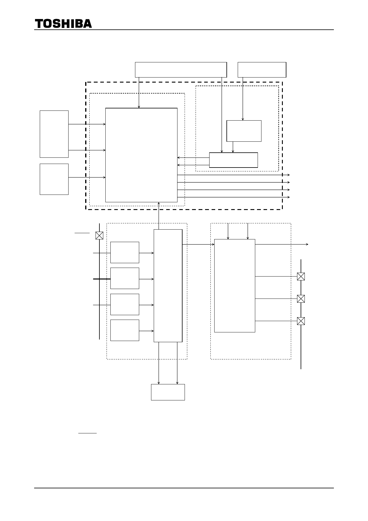
4. Output control circuit, current feedback circuit and current setting circuit (A/B unit
(C/D unit is the same as A/B unit)
Micro-step current setting
data logic circuit
Chopping
reference circuit
Current
feedback
circuit
Current
setting
circuit
Output control circuit PHASE
NF
set current
reached signal
RNF
set current
monitor signal
MIXED
DECAY
TIMING
Charge start
Output stop
signal
Output control circuit
U1
U2
L1
L2
DECAY
MODE
MIXED
DECAY
TIMING
circuit
CR
COUNTER
CR COUNTER
Output circuit
RESET
Output pin
VM
VDD
ISD (current
shutdown)
circuit
VMR
circuit
VDDR
circuit
Output RESET signal
Reset signal
selector
circuit
Charge
pump
halt
signal
VDD
VM
Power supply
for upper
output MOS
transistors
VH
Charge pump
circuit
Thermal
shut down
(TSD)
circuit
Protection circuit
Charge pump
circuit
MICRO-STEP
CURRENT SETUP
LATCH CLEAR signal
VDDR: VDD power on Reset
VMR: VM power on Reset
ISD: Current shutdown circuit
TSD: Thermal shutdown circuit
LOGIC
MIXED DECAY
TIMING TABLE
CLEAR signal
Output
circuit
Ccp A
Ccp B
Ccp C
Note: The RESET pins is pulled down in the IC by 10-kΩ resistor.
When not using the pin, connect it to GND. Otherwise, malfunction may occur.
www.DataSheet4U.com
5 2005-04-04
5 Page 
www.DataSheet4U.com
TB62202AFG
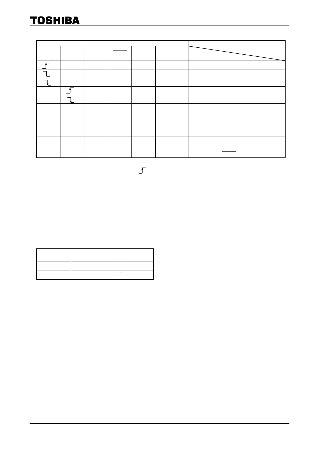
2. Serial input signal functions
Input
CLK STROBE DATA RESET
× ×H
× HH
× LH
× ×H
× ×H
×××L
××××
× × ×H
VDDR
(Note 1) or
VMR
H
H
H
H
H
×
L
H
Operation of
TSD/ISD
L
L
L
L
L
L
L
H
(Note 2)
Action
No change in shift register.
H level is input to shift register.
L level is input to shift register.
Shift register data are latched.
Qn
Output off, charge pump halted
(S/R DATA CLR)
Output off (S/R DATA CLR)
Charge pump halted
Mixed decay timing table cleared (only VDDR)
Output off (S/R DATA HOLD)
Charge pump halted
Restored when RESET goes from Low to High
×: Don’t Care
Qn: Latched output level when STROBE is .
Note 1: VDDR and VMR
H when the operable range (3 V typical) or higher and L when lower.
When one of VDDR or VMR is operating, the system resets (OR relationship).
Note 2: High when TSD is in operation.
When one of TSD or ISD is operating, the system resets (OR relationship).
Note: Function of overcurrent protection circuit
Until the RESET signal is input after ISD is triggered, the overcurrent protection circuit remains in operation.
During ISD, the charge pump stays halted.
When TSD and ISD are operating, the charge pump halts.
3. PHASE functions
Input
H
L
Function
Positive polarity (A: H, Α : L)
Negative polarity (A: L, Α : H)
www.DataSheet4U.com
11
2005-04-04
11 Page | ||
| Páginas | Total 30 Páginas | |
| PDF Descargar | [ Datasheet TB62202AFG.PDF ] | |
Hoja de datos destacado
| Número de pieza | Descripción | Fabricantes |
| TB62202AFG | Dual-Stepping Motor Driver IC | Toshiba Semiconductor |
| Número de pieza | Descripción | Fabricantes |
| SLA6805M | High Voltage 3 phase Motor Driver IC. |
Sanken |
| SDC1742 | 12- and 14-Bit Hybrid Synchro / Resolver-to-Digital Converters. |
Analog Devices |
|
DataSheet.es es una pagina web que funciona como un repositorio de manuales o hoja de datos de muchos de los productos más populares, |
| DataSheet.es | 2020 | Privacy Policy | Contacto | Buscar |
