|
|
|
PDF EDGE720 Data sheet ( Hoja de datos )
| Número de pieza | EDGE720 | |
| Descripción | 500Mhz Pin Electronics Driver | |
| Fabricantes | Semtech Corporation | |
| Logotipo | ||
Hay una vista previa y un enlace de descarga de EDGE720 (archivo pdf) en la parte inferior de esta página. Total 30 Páginas | ||
|
No Preview Available !
Edge720
U.com 5W00indMoHwz CPoinmEplaercattroorn,icasndDrLioveard,TEST AND MEASUREMENT PRODUCTS
t4Description
Features
eeThe Edge720 is a totally monolithic ATE pin electronics
Shsolution manufactured in a high-performance
tacomplementary bipolar process.
.DaThe three-statable driver is capable of generating 9V
swings over a –1V to +12V range. In addition, 13V super
wvoltage may be obtained under certain operating
wconditions. An input power down mode allows extremely
wlow leakage current in HiZ. Thus, the Edge720 can help
mto eliminate relays that are typically used to isolate devices
osuch as per pin measurement units from the driver/
comparator/load.
.cThe load supports programmable source and sink currents
Uof ± 35 mA over a –1V to +12V range, or it can be
completely disabled. In addition, the load is configurable
t4and may be used as a programmable voltage clamp.
• Fully Integrated Three-Statable Driver, Window
Comparator, and Dynamic Active Load
• 13V Driver, Load, Compare Range
• +13V Super Voltage Capable
• ± 35 mA Programmable Load
• Comparator Input Tracking >6V/ns
• Leakage (L+D+C) < 2 µA (normal mode, typical)
• Leakage (L+D+C) < 30 nA (power-down mode,
guaranteed)
• Small footprint (52 lead Exposed Pad QFP)
Applications
• Flash Memory Test
• VLSI Test Equipment
• Mixed-Signal Test Equipment
• Memory Testers (Bidirectional Channels)
• ASIC Verifiers
eThe window comparator spans a 13V common mode
range, tracks input signals with edge rates greater than 6
eV/ns and passes sub-ns pulses. An input power down
hmode allows for extremely low leakage measurements.
SThe inclusion of all pin electronics building blocks into a
ta52 lead QFP (10 mm body w/ exposed heat sink) offers a
highly integrated solution that is traditionally implemented
with multiple integrated circuits or discretes.
aThe Edge720 is a variant of the Edge710, with the
.Dfollowing improvements:
w• Reduced D+C+L Leakage Current
• Increased Super Voltage Range
w• Additional VCM_IN buffer reduces the need for
an external buffer when using the load circuit as
w oma programmable clamp.
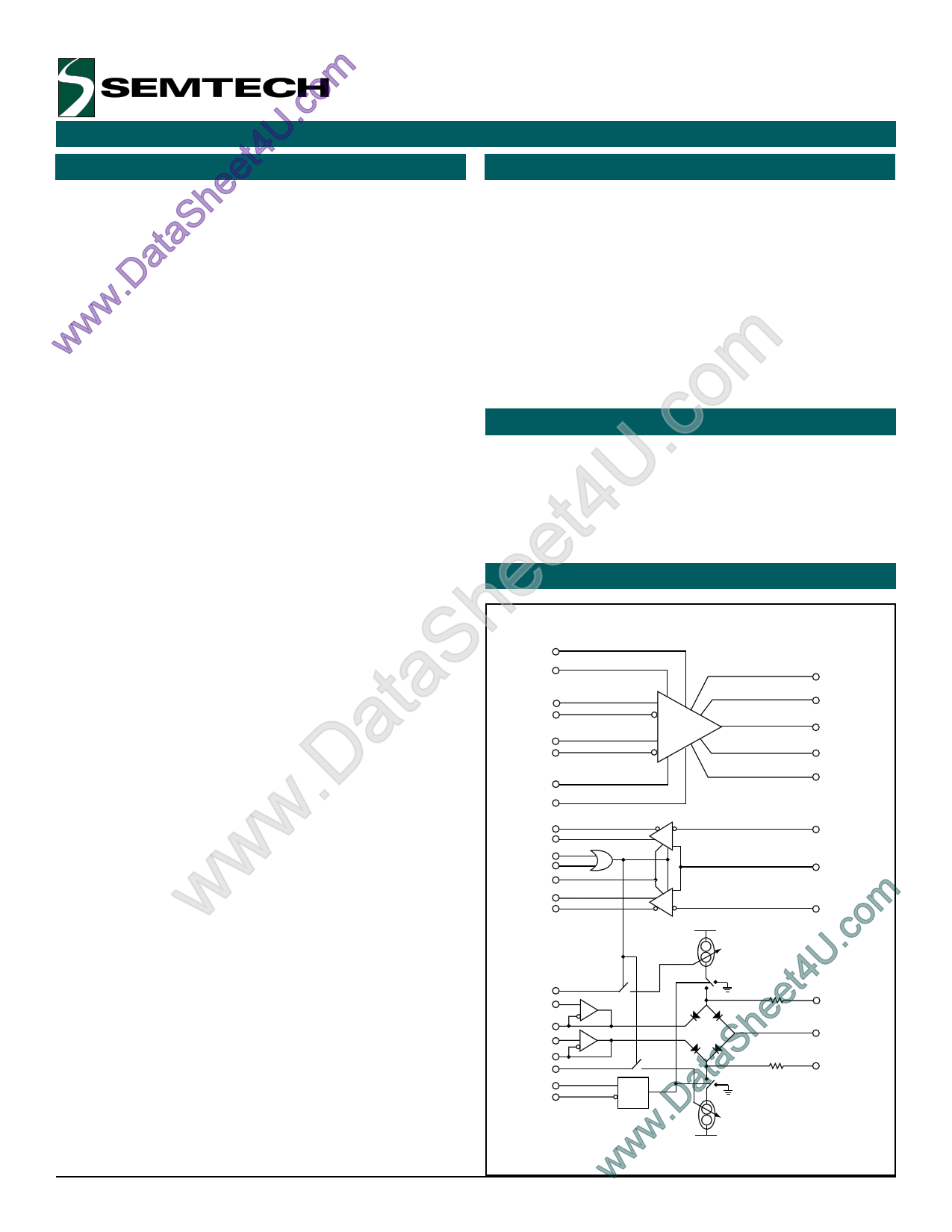
Functional Block Diagram
BIAS
DVH
DHI
DHI*
DVR_EN
DVR_EN*
DVL
IPD_D
QA*
QA
IPD_C
SUPERV
PECL
QB
QB*
VCC
DVH_CAP
RADJ
DOUT
FADJ
DVL_CAP
CVA
VINP
CVB
.cISC
t4UISC_IN
eVCM_IN_A
eVCM_OUT_A
hVCM_IN_B
SVCM_OUT_B
taISK_IN
LD_EN
www.DaLD_EN*
ISK
VEE
BRIDGE_SC
LOAD
BRIDGE_SK
Revision 4 / October 3, 2002
1
www .semtech.com
1 page 
Edge720
TEST AND MEASUREMENT PRODUCTS
Circuit Description
Driver Circuit Description
Driver Enable Inputs (DRV_EN(*))
Introduction
The Edge720 features a driver circuit that can be used to
drive voltage levels over a –1V to +12V range at
frequencies of up to 500 MHz at the DOUT pin. In addition,
the driver can be used to force a super voltage level of up
to 13V and can also be placed in a high impedance state.
The driver circuit of the Edge720 is a variant of the driver
circuit of the Edge710, and was specifically designed to
offer a low leakage solution to FLASHTM memory testing..
A block diagram of the driver can be seen in Figure 1.
The driver enable inputs, DRV_EN(*), control whether the
driver is forcing a voltage at DOUT, or is placed in a high
impedance state. If the voltage applied to DRV_EN is
more positive than that applied to DRV_EN*, the driver,
will force the DOUT voltage to either DVH or DVL
(determined by DHI(*)). If the voltage applied to DRV_EN
is less than that applied to DRV_EN*, the driver will force
the DOUT pin to a high impedance state (see Table 2 for
DRV_EN(*) functionality). It is important to note that for
predictable operation, DRV_EN(*) pins must not be left
floating.
BIAS
DVH
DHI
DHI*
DVR_EN
DVR_EN*
DVL
IPD_D
DVH_CAP
RADJ
DOUT
FADJ
DVL_CAP
Figure 1. Block Diagram of the Edge720 Driver
Driver Enable
DRV_EN > DRV_EN*
DRV_EN > DRV_EN*
DRV_EN < DRV_EN*
Driver Data
DHI > DHI*
DHI < DHI*
X
DOUT
DVH
DVL
HiZ
Table 2. DRV_EN(*) and DHI(*)
Control Input Functionality
Input Power Down
Driver Digital “Flex-In” Inputs
The Edge720 driver circuit features “Flex-In” control inputs
for the driver enable (DRV-EN(*)) and driver data (DHI(*))
inputs that allow the driver to receive ECL, TTL, CMOS, or
custom signal levels. These “Flex-In” inputs are wide
voltage differential inputs whose operation is described in
Table 1.
The driver input power down pin, IPD_D, is a TTL compatible
input that can be used to place the driver in input power
down (IPD) mode. IPD_D functionality is described below
in Table 3.
IPD_D
0
Operation
Normal
Min Max Units
Common Mode Input Range VEE + 2.75 5.0
V
1 IPD Mode
Table 3. IPD_D Functionality
Differential Input Range
±0.25 ±4.0 V
Table 1. “Flex-In” Input Characteristics
Single-ended operation of these inputs can be
accomplished by connecting the inverting input (DHI* or
DRV_EN*) to the desired DC threshold level.
IPD mode should be invoked when the driver is in high
impedance mode (DRV_EN < DRV_EN*). When in IPD
mode, the driver output leakage will be minimized. It is
important to note that IPD_D should not be left floating.
If IPD_D is not being used, it should be connected to GND.
Revision 4 / September 24, 2002
5
www .semtech.com
5 Page 
Edge720
TEST AND MEASUREMENT PRODUCTS
Circuit Description (continued)
Load Circuit Description
Current Programming Inputs
Introduction
The Edge720 features a programmable load circuit which
is capable of sourcing or sinking up to 35 mA over a –1V
to +12V range, or being placed in a high impedance state.
This circuit also features “split” commutating voltage inputs
that allow it to be configured as a programmable voltage
clamp. In addition, the BRIDGE_SC and BRIDGE_SK pins
allow the load circuit’s diode bridge to be connected to
external current sources for increased low current accuracy.
A functional schematic of the Edge720’s load circuit can
be seen below in Figure 12.
IPD_C
SUPERV
ISC_IN
VCC
ISC
VCM_IN_A
VCM_OUT_A
VCM_OUT_B
VCM_IN_B
ISK_IN
LD_EN
LD_EN*
1 KΩ
1 KΩ
BRIDGE_SC
LOAD
BRIDGE_SK
ISK
VEE
Figure 12. Functional Schematic of the
Edge720’s Load Circuit
Load Enable
The Edge720 load circuit features a differential “Flex In”
input labeled LD_EN(*). This input can be used to isolate
the diode bridge from the on-chip current supplies, leaving
the LOAD pin in a high impedance state. “Flex In” inputs
are wide voltage inputs which allow the LD_EN(*) pin to
be used with ECL, TTL, CMOS, or custom level inputs, and
whose characteristics are described in Table 1. LD_EN(*)
functionality is described in Table 6.
ISC_IN and ISK_IN are independently adjustable analog
current inputs that control the amount of current being
supplied to the diode bridge by the on-chip current supplies
(see Figure 12). Consequently, these inputs can be used
to program the amount of current being sourced (ISC_IN)
or sunk (ISK_IN) at the load circuit output pin (LOAD).
The on-chip current supplies have been designed to have
a nominal gain of 20. Therefore, the magnitude of current
sourced or sunk is equal to the magnitude of the control
current scaled by a factor of 20. The ISK_IN and ISC_IN
current programming inputs should be routed on a PCB
such that coupling between the control inputs and the
LOAD, VCM_OUT_A and VCM_OUT_B pins is minimized.
Finally, it is also recommended that 1 kΩ of external series
resistance be connected between these inputs and the
source controlling them. A group E DAC on the Edge6420
offers a nice solution to controlling these inputs.
Commutating Voltage Inputs
VCM_IN_A(B) are high impedance analog voltage inputs
to on-chip buffers that are used to set the voltage level at
which the diode bridge switches from sourcing to sinking
current when the load is connected as a standard active
load (see Figure 15). If the voltages applied to
VCM_IN_A(B) are more positive than that on the LOAD
pin, the bridge will source current from the LOAD pin (see
Figure 13). If the voltage applied to VCM_IN_A(B) is less
than that at the LOAD pin, the bridge will sink current
through the LOAD pin (see Figure 14).
VCM_IN_A
External
Connection
VCM_IN_B
LOAD
VCM_IN_A(B) > LOAD
Load Enable Input
Operation
Figure 13. Edge720 Load Circuit Sources Current
LD_EN < LD_EN*
LD_EN > LD_EN*
High Impedance
Active
Table 6. Load Enable Input Functionality
VCM_IN_A
External
Connection
VCM_IN_B
LOAD
Single-ended operation can be attained by connecting the
inverting input, LD_EN* to the desired DC threshold level.
Revision 4 / September 24, 2002
11
VCM_IN_A(B) < LOAD
Figure 14. Edge720 Load Circuit Sinks Current
www .semtech.com
11 Page | ||
| Páginas | Total 30 Páginas | |
| PDF Descargar | [ Datasheet EDGE720.PDF ] | |
Hoja de datos destacado
| Número de pieza | Descripción | Fabricantes |
| EDGE720 | 500Mhz Pin Electronics Driver | Semtech Corporation |
| EDGE728 | Very High Speed Dual and Quad Channel ECL Delay Lines | Semtech Corporation |
| Número de pieza | Descripción | Fabricantes |
| SLA6805M | High Voltage 3 phase Motor Driver IC. |
Sanken |
| SDC1742 | 12- and 14-Bit Hybrid Synchro / Resolver-to-Digital Converters. |
Analog Devices |
|
DataSheet.es es una pagina web que funciona como un repositorio de manuales o hoja de datos de muchos de los productos más populares, |
| DataSheet.es | 2020 | Privacy Policy | Contacto | Buscar |