|
|
|
PDF RC4391 Data sheet ( Hoja de datos )
| Número de pieza | RC4391 | |
| Descripción | Inverting And Step-down Switching Regulator | |
| Fabricantes | Fairchild Semiconductor | |
| Logotipo | ||
Hay una vista previa y un enlace de descarga de RC4391 (archivo pdf) en la parte inferior de esta página. Total 22 Páginas | ||
|
No Preview Available !
www.fairchildsemi.com
RC4391
Inverting and Step-Down Switching Regulator
Features
• Versatile —
Inverting function (+ to -)
Step-down function
Adjustable output voltage
Regulates supply changes
• Micropower —
Low quiescent current — 170 mA
Wide supply range — 4V to 30V
• High performance —
High switch current — 375 mA
High efficiency — 70% typically
• Low battery detection capability
• 8-lead mini-DIP or S.O. package
Description
Fairchild Semiconductor’s RC4391 is a monolithic switch
mode power supply controller for micropower circuits. The
RC4391 integrates all the active functions needed for low
power switching supplies, including oscillator, switch, refer-
ence and logic, into a small package. Also, the quiescent
supply current drawn by the RC4391 is extremely low; this
combination of low supply current, function, and small pack-
age make it adaptable to a variety of miniature power supply
applications.
The RC4391 complements another Fairchild Semiconductor
switching regulator IC, the RC4190. The RC4190 is dedi-
cated to step-up (VOUT > VIN) applications, while the
RC4391 was designed for inverting (VOUT = -VIN) and
step-down (VOUT < VIN) applications. Between the two
devices the ability to create all three basic switching regula-
tor configurations is assured. Refer to the RC4190 data sheet
for information on step-up applications.
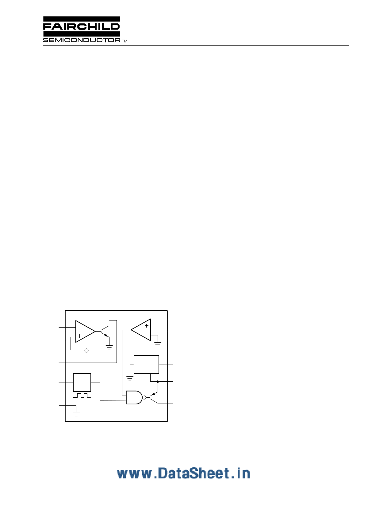
The functions provided are:
Block Diagram
RC4391
LBR
C2
Q2
C1
• Squarewave oscillator (adjustable externally)
• Bandgap voltage reference
• High current PNP switch transistor
• Feedback comparator
• Logic for gating the comparator
VFB • Circuitry for detecting a discharged battery condition
(in battery powered systems)
LBD
CX
Gnd
VREF
OSC
+1.25V
REF/Bias
Q1
Few external components are required to build a complete
DC-to-DC converter:
VREF
• Inductor
+VS • Low value capacitor to set the oscillator frequency
• Electrolytic filter capacitor
• Steering diode
CX • Two resistors
65-3471-01
Rev. 1.1.1
1 page 
RC4391
Typical Performance Characteristics
6.5
6.0
5.5
5.0
4.5
4.0
3.5
3.0
0
5 10 15 20 25
+VS (V)
Figure 1. Oscillator Frequency vs. Supply Voltage
PRODUCT SPECIFICATION
8
7
6
5
4
3
2
1
0
-55 0
25 70 125
TA (¡C)
Figure 2. Oscillator Frequency vs. Temperature
1.260
1.255
1.250
1.245
1.240
-55 0
25 70 125
TA (¡C)
Figure 3. Reference Voltage vs. Temperature
1.260
1.255
1.250
1.245
1.240
4 6 10 20 30
+VS (V)
Figure 4. Reference Voltage vs. Supply Voltage
600
500
400
300
200
100
20
10
0
1
2 3 4 567
VCE (SAT) (V)
8
Figure 5. Collector Current vs. Q1 Saturation Voltage
4
3
2
1
0
-55 0
25 70 125
TA (¡C)
Figure 6. Minimum Supply Voltage vs. Temperature
5
5 Page 
RC4391
PRODUCT SPECIFICATION
Device Shutdown
The entire device may be shut down to an extremely low cur-
rent non-operating condition by disconnecting the ground
(pin 4). This can be easily done by putting an NPN transistor
in series with ground pin and switching it with an external
signal. This switch will not affect the efficiency of operation,
but will add to and increase the reference voltage by an
amount equal to the saturation voltage of the transistor used.
A mechanical switch can also be used in series between
circuit ground and pin 4, without introducing any reference
offset.
Power Transistor Interfaces
The most important consideration in selecting an external
power transistor is the saturation voltage at IC = IMAX.
The lower the saturation voltage is, the better the efficiency
will be. Also, a higher beta transistor requires less base drive
and therefore less power will be.
Also, a higher beta transistor requires less base drive and
therefore less power will be consumed in driving it, improv-
ing efficiency losses in the interface. The part numbers given
in the following applications are recommended, but other
types may be more appropriate depending on voltage and
power levels.
When troubleshooting external power transistor circuits,
ensure that clean, sharp-edged waveforms are driving the
interface and power transistors. Monitor these waveforms
with an oscilloscop—disconnect the inductor, and tie the
VFB input (pin 8) high through a 10K resistor. This will
cause the regulator to pulse at maximum duty cycle without
drawing excessive inductor currents. Check for expected on
time and off time, and look for slow rise times that might
cause the power transistor to enter its linear operating region.
The following external power transistor circuits may demand
some adjustment to resistor values to satisfy various power
levels and input/output voltages. CX and LX values must be
selected according to the design equations (pages 2-213 and
2-214).
Inverting Medium Power Application
Figure 8 is a schematic of an inverting medium power supply
(250mW to 1W) using an external PNP switch transistor.
Supply voltage is applied to the IC via R3: when the internal
switch transistor is turned on current through R4 is also
drawn through R3; creating a voltage drop from base to
emitter of the external switch transistor. This drop turns on
the external transistor.
Voltage pulses on the supply lead (pin 6) do not affect circuit
operation because the internal reference and bias circuitry
have good supply rejection capabilities. A power Schottky
diode is used for higher efficiency.
Inverting High Power Application
For higher power applications (500mW to 5W), refer to
Figure 9. This circuit uses an extra external transistor to pro-
vide well controlled drive current in the correct phase to the
power switch transistor. The value of R3 sets the drive
current to the switch by making the interface transistor act as
a current source. R4 and R5 must be selected such that the
RC time constant of R4 and the base capacitance of Q2 do
not slow the response time (and affect duty cycle), but not so
low in value that excess power is consumed and efficiency
suffers. The resistor values chosen should be proportional to
the supply voltage (values shown are for +5V).
Step-Down Power Applications
Figures 16 and 17 show medium and high power interfaces
modified to perform step-down functioning. The design
+5V
C1
0.1µF
R2
62 k½
R3
1k½
5 7 65
VFB VREF +Vs L x
4391
Cx
3
150 pF
Cx
GND
4
Q1
2N3635
Motorola
MBR030
R4
50½ 220µH
-24V
CF
100µF
R1
1.2 M½
65-2476
Figure 14. Inverting Medium Power Application
11
11 Page | ||
| Páginas | Total 22 Páginas | |
| PDF Descargar | [ Datasheet RC4391.PDF ] | |
Hoja de datos destacado
| Número de pieza | Descripción | Fabricantes |
| RC4391 | Inverting And Step-down Switching Regulator | Fairchild Semiconductor |
| Número de pieza | Descripción | Fabricantes |
| SLA6805M | High Voltage 3 phase Motor Driver IC. |
Sanken |
| SDC1742 | 12- and 14-Bit Hybrid Synchro / Resolver-to-Digital Converters. |
Analog Devices |
|
DataSheet.es es una pagina web que funciona como un repositorio de manuales o hoja de datos de muchos de los productos más populares, |
| DataSheet.es | 2020 | Privacy Policy | Contacto | Buscar |