|
|
PDF ADS1207 Data sheet ( Hoja de datos )
| Número de pieza | ADS1207 | |
| Descripción | (ADS1206 / ADS1207) LOW-POWER / SYNCHRONOUS VOLTAGE-TO-FREQUENCY CONVERTER | |
| Fabricantes | Burr-Brown Corporation | |
| Logotipo |  |
|
Hay una vista previa y un enlace de descarga de ADS1207 (archivo pdf) en la parte inferior de esta página. Total 8 Páginas | ||
|
No Preview Available !
LowĆPower, Synchronous
VoltageĆtoĆFrequency Converter
ADS1206
ADS1207
SBAS311 − MARCH 2004
FEATURES
D Syncronous Operation
D Frequency Set By External Clock
D Maximum Input Frequency:
− 1MHz for ADS1206
− 4MHz for ADS1207
D Selectable High-Impedance Buffered Input
D 2% Internal, 2.5V Reference Voltage
D High-Current Output Driver
D Power Supply 3.3V or 5V
D Low Power : 3mW (typ)
D Alternate Source for AD7740
D −40°C to +85°C Operating Temperature Range
APPLICATIONS
D Galvanic Isolation Measurement
D High Voltage Measurement
D Low-Cost Analog-to-Digital Conversion
D Motor Control
D Industrial Process Control
D Instrumentation
D Smart Transmitters
D Portable Instruments
DESCRIPTION
The ADS1206 and ADS1207 are a low-cost,
high-performance, synchronous voltage-to-frequency
converters (VFC). Both devices can operate from a single
3.0V to 3.6V or 4.5V to 5.5V power supply, consuming only
1mA. The output signal is synchronous with the input
clock, CLKIN. The clock input is TTL- and CMOS-
compatible and the onboard clock generator can also
accept an external crystal or resonator. The maximum
input clock frequency for the ADS1206 is 1MHz and for the
ADS1207 is 4MHz. The clock divider on the ADS1207
scales the input frequency to 2MHZ, which permits the
core to operate at the higher rate. The high-impedance
input is ideal for direct connection to high-impedance
transducers or high-voltage resistive dividers. Counting
output pulses over a 4ms period results in an effective
12-bit resolution for the ADS1206 using a 1MHz input
clock. For the ADS1207 using a 4MHz input clock, the
same result occurs over a 2ms period. Both devices are
designed for use in medium-resolution measurements.
They are available in an 8-lead VSSOP package.
REFIN/OUT
1kΩ Reference
Voltage
2.5V
VIN x1
Modulator
Buffer
FOUT
BUF
−2
ADS1207
Only
CLKOUT
CLKIN
Please be aware that an important notice concerning availability, standard warranty, and use in critical applications of Texas Instruments
semiconductor products and disclaimers thereto appears at the end of this data sheet.
All trademarks are the property of their respective owners.
PRODUCT PREVIEW information concerns products in the formative or design
phase of development. Characteristic data and other specifications are design
goals. Texas Instruments reserves the right to change or discontinue these
products without notice.
www.ti.com
Copyright 2004, Texas Instruments Incorporated
1 page 
www.ti.com
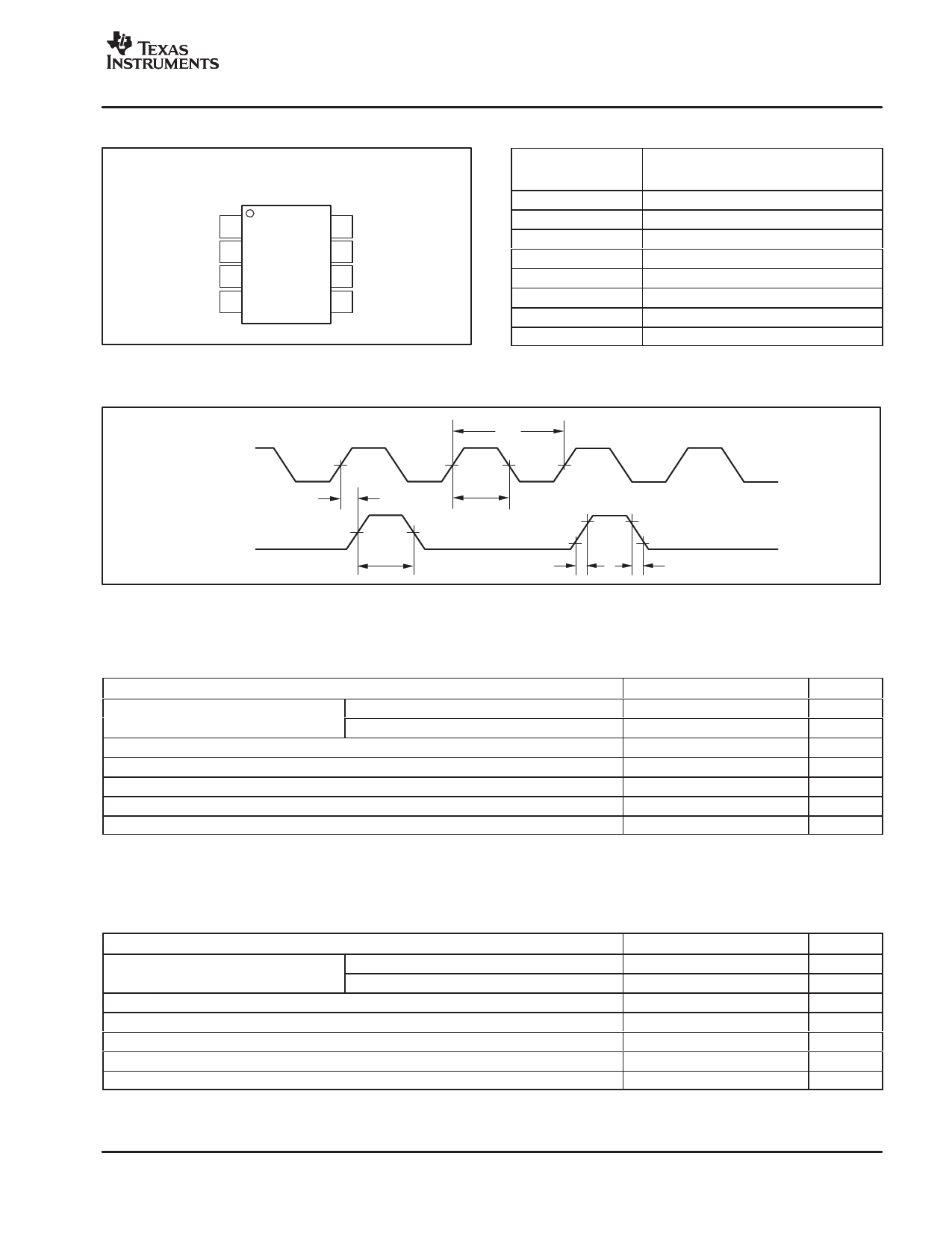
PIN ASSIGNMENTS
VSSOP PACKAGE
(TOP VIEW)
CLKOUT 1
CLKIN 2
GND 3
REFIN/OUT 4
8 BUF
7 FOUT
6 VDD
5 VIN
ADS1206
ADS1207
SBAS311 − MARCH 2004
Terminal Functions
TERMINAL
NAME
NO.
CLKOUT
1
CLKIN
2
GND
3
REFIN/OUT
4
VIN 5
VDD
FOUT
6
7
BUF
8
DESCRIPTION
Clock output
Master clock input
Ground
Reference voltage input or output
Analog input
Power supply, +3.3V or +5V nominal
Modulator output
Buffered mode select
PARAMETER MEASUREMENT INFORMATION
CLKIN
FOUT
tD1
tW2
tC1
tW1
tR1
tF1
Figure 1. Timing Diagram
TIMING REQUIREMENTS: 5.0V
over recommended operating free-air temperature range at −40°C to +85°C,, and VDD = 5V, unless otherwise noted.
PARAMETER
MIN MAX UNITS
tC1 Input clock period
ADS1206
ADS1207
1000
250
TBD
TBD
ns
ns
tW1 Input clock high time
tD1 FOUT rising edge delay after input clock rising edge
(tC1/2) − 100 (tC1/2) + 100
TBD
TBD
ns
ns
tW2 FOUT high time
tR1 FOUT rise time
tC1 − 20
TBD
tC1 + 20
TBD
ns
ns
tF1 FOUT fall time
TBD
TBD
ns
NOTE: Applicable for 5.0V nominal supply: VDD (min) = 4.5V and VDD (max) = 5.5V. All input signals are specified with tR = tF = 5ns (10% to 90%
of VDD) and timed from a voltage level of (VIL + VIH)/2. See timing diagram.
TIMING REQUIREMENTS: 3.3V
over recommended operating free-air temperature range at −40°C to +85°C,, and VDD = 3.3V, unless otherwise noted.
PARAMETER
MIN MAX UNITS
tC1 Input clock period
ADS1206
ADS1207
1000
250
TBD
TBD
ns
ns
tW1 Input clock high time
(tC1/2) − 100 (tC1/2) + 100
ns
tD1 FOUT rising edge delay after input clock rising edge
TBD
TBD
ns
tW2 FOUT high time
tC1 − 8
tC1 + 8
ns
tR1 FOUT rise time
TBD
TBD
ns
tF1 FOUT fall time
TBD
TBD
ns
NOTE: Applicable for 3.3V nominal supply: VDD (min) = 3.0V and VDD (max) = 3.6V. All input signals are specified with tR = tF = 5ns (10% to 90%
of VDD) and timed from a voltage level of (VIL + VIH)/2. See timing diagram.
5
5 Page | ||
| Páginas | Total 8 Páginas | |
| PDF Descargar | [ Datasheet ADS1207.PDF ] | |
Hoja de datos destacado
| Número de pieza | Descripción | Fabricantes |
| ADS1201 | High Dynamic Range DELTA-SIGMA MODULATOR | Burr-Brown Corporation |
| ADS1201 | High Dynamic Range Delta-Sigma Modulator | Texas Instruments |
| ADS1201U | High Dynamic Range DELTA-SIGMA MODULATOR | Burr-Brown Corporation |
| ADS1202 | Motor Control Current Shunt 1-Bit/ 10MHz/ 2nd-Order/ Delta-Sigma Modulator | Burr-Brown Corporation |
| Número de pieza | Descripción | Fabricantes |
| SLA6805M | High Voltage 3 phase Motor Driver IC. |
Sanken |
| SDC1742 | 12- and 14-Bit Hybrid Synchro / Resolver-to-Digital Converters. |
Analog Devices |
|
DataSheet.es es una pagina web que funciona como un repositorio de manuales o hoja de datos de muchos de los productos más populares, |
| DataSheet.es | 2020 | Privacy Policy | Contacto | Buscar |
