|
|
|
PDF ADR512 Data sheet ( Hoja de datos )
| Número de pieza | ADR512 | |
| Descripción | 1.2 V Precision Low Noise Shunt Voltage Reference | |
| Fabricantes | Analog Devices | |
| Logotipo | ||
Hay una vista previa y un enlace de descarga de ADR512 (archivo pdf) en la parte inferior de esta página. Total 8 Páginas | ||
|
No Preview Available !
1.2 V Precision Low Noise
Shunt Voltage Reference
ADR512
FEATURES
Precision 1.200 V Voltage Reference
Ultracompact 3 mm ؋ 3 mm SOT-23 Package
No External Capacitor Required
Low Output Noise: 4 V p-p (0.1 Hz to 10 Hz)
Initial Accuracy: ؎0.3% Max
Temperature Coefficient: 60 ppm/؇C Max
Operating Current Range: 100 A to 10 mA
Output Impedance: 0.3 ⍀ Max
Temperature Range: –40؇C to +85؇C
APPLICATIONS
Precision Data Acquisition Systems
Battery-Powered Equipment:
Cellular Phone, Notebook Computer, PDA,
and GPS
3 V/5 V, 8-/12-Bit Data Converters
Portable Medical Instruments
Industrial Process Control Systems
Precision Instruments
GENERAL DESCRIPTION
Designed for space critical applications, the ADR512 is a low
voltage (1.200 V), precision shunt-mode voltage reference in the
ultracompact (3 mm ϫ 3 mm) SOT-23 package. The ADR512
features low temperature drift (60 ppm/ЊC), high accuracy
(Ϯ0.30%), and ultralow noise (4 V p-p) performance.
The ADR512’s advanced design eliminates the need for an
external capacitor, yet it is stable with any capacitive load. The
minimum operating current increases from a scant 100 A to a
maximum of 10 mA. This low operating current and ease of use
make the ADR512 ideally suited for handheld battery-powered
applications.
PIN CONFIGURATION
3-Lead SOT-23
V+ 1
V– 2
ADR512
3 TRIM/NC
ADR512
Model
ADR512ART-REEL7
Output
Voltage
(VO)
1.200
Initial
Accuracy
(mV) (%)
3.5 0.3
Temperature
Coefficient
(ppm/؇C)
60
A TRIM terminal is available on the ADR512 to provide adjust-
ment of the output voltage over Ϯ0.5% without affecting the
temperature coefficient of the device. This feature provides
users with the flexibility to trim out any system errors.
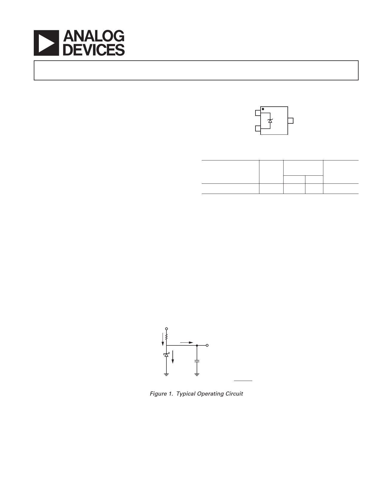
IL + IQ
VS
RBIAS
ADR512
IQ
IL
VOUT = 1.2V
COUT
(OPTIONAL)
VS – VOUT
RBIAS = IL + IQ
Figure 1. Typical Operating Circuit
REV. 0
Information furnished by Analog Devices is believed to be accurate and
reliable. However, no responsibility is assumed by Analog Devices for its
use, nor for any infringements of patents or other rights of third parties that
may result from its use. No license is granted by implication or otherwise
under any patent or patent rights of Analog Devices. Trademarks and
registered trademarks are the property of their respective companies.
One Technology Way, P.O. Box 9106, Norwood, MA 02062-9106, U.S.A.
Tel: 781/329-4700
www.analog.com
Fax: 781/326-8703 © 2003 Analog Devices, Inc. All rights reserved.
1 page 
ADR512
Adjustable Precision Voltage Source
The ADR512, combined with a precision low input bias op amp
such as the AD8610, can be used to output a precise adjustable
voltage. Figure 2 illustrates the implementation of this application
using the ADR512.
The output of the op amp, VOUT, is determined by the gain of the
circuit, which is completely dependent on resistors R2 and R1.
VOUT
=1+
R2
R1
(4)
An additional capacitor in parallel with R2 can be added to filter
out high frequency noise. The value of C2 is dependent on the
value of R2.
VCC
RBIAS
1.2V
AD8610
VOUT = 1.2(1 + R2/R1)
ADR512
R2
R1 C2 (OPTIONAL)
Figure 2. Adjustable Precision Voltage Source
Output Voltage Trim
Using a mechanical or digital potentiometer, the output voltage
of the ADR512 can be trimmed ± 0.5%. The circuit in Figure 3
illustrates how the output voltage can be trimmed, using a 10 kΩ
potentiometer.
VCC
RBIAS
ADR512
R1
100k⍀
VOUT
POT
50k⍀
Figure 3. Output Voltage Trim
Using the ADR512 with Precision Data Converters
The compact ADR512 package and the device’s low minimum
operating current requirement make it ideal for use in battery-
powered portable instruments, such as the AD7533 CMOS
multiplying DAC, that use precision data converters.
Figure 4 shows the ADR512 serving as an external reference to
the AD7533, a CMOS multiplying DAC. Such a DAC requires
a negative voltage input in order to provide a positive output
range. In this application, the ADR512 is supplying a –1.2 V
reference to the REF input of the AD7533.
ADR512
R2
0
MSB
VDD
1
9
LSB
AD7533
1
GN
32 1
15
–VDD
VOUT = 0V TO 1.2V
Figure 4. ADR512 as a Reference for a 10-Bit
CMOS DAC (AD7533)
Precise Negative Voltage Reference
The ADR512 is suitable for use in applications where a precise
negative voltage reference is desired, including the application
detailed in Figure 4.
Figure 5 shows the ADR512 configured to provide a –1.2 V output.
ADR512 –
R1
–1.2V
–VDD
Figure 5. Precise –1.2 V Reference Configuration
Since the ADR512 characteristics resemble those of a Zener diode,
the cathode shown in Figure 5 will be 1.2 V higher with respect
to the anode (V+ with respect to V– on the ADR512 package).
Since the cathode of the ADR512 is tied to ground, the anode
must be –1.2 V.
R1 in Figure 5 should be chosen so that 100 µA to 10 mA is
provided to properly bias the ADR512.
R1 = VDD
I
(5)
The resistor R1 should be chosen so that power dissipation is at
a minimum. An ideal resistor value can be determined through
manipulation of Equation 5.
REV. 0
–5–
5 Page | ||
| Páginas | Total 8 Páginas | |
| PDF Descargar | [ Datasheet ADR512.PDF ] | |
Hoja de datos destacado
| Número de pieza | Descripción | Fabricantes |
| ADR510 | 1.0 V Precision Low Noise Shunt Voltage Reference | Analog Devices |
| ADR512 | 1.2 V Precision Low Noise Shunt Voltage Reference | Analog Devices |
| Número de pieza | Descripción | Fabricantes |
| SLA6805M | High Voltage 3 phase Motor Driver IC. |
Sanken |
| SDC1742 | 12- and 14-Bit Hybrid Synchro / Resolver-to-Digital Converters. |
Analog Devices |
|
DataSheet.es es una pagina web que funciona como un repositorio de manuales o hoja de datos de muchos de los productos más populares, |
| DataSheet.es | 2020 | Privacy Policy | Contacto | Buscar |