|
|
|
PDF CH7013B Data sheet ( Hoja de datos )
| Número de pieza | CH7013B | |
| Descripción | Digital PC to TV Encoder | |
| Fabricantes | Chrontel | |
| Logotipo | ||
Hay una vista previa y un enlace de descarga de CH7013B (archivo pdf) en la parte inferior de esta página. Total 30 Páginas | ||
|
No Preview Available !
CCCCHHHRhRROrOoONNnNTTTtEeEELlLL
Digital PC to TV Encoder
CH7013B
1. FEATURES
• Universal digital interface accepts YCrCb (CCIR601
or 656) or RGB (15, 16 or 24-bit) video data in both
non-interlaced and interlaced formats
• True scale rendering engine supports underscan
operations for various graphics resolutions
• Enhanced text sharpness and adaptive flicker removal
with up to 5-lines of filtering
• Enhanced dot crawl control and area reduction
• Fully programmable through serial port
• Supports NTSC, NTSC-J, and PAL (B, D, G, H, I, M
and N) TV formats
• Provides Composite, S-Video and SCART outputs
• Auto-detection of TV presence
• Supports VBI pass-through
• Programmable power management
• 9-bit video DAC outputs
• Complete Windows and DOS driver software
• Offered in 48-pin LQFP
2. GENERAL DESCRIPTION
Chrontel’s CH7013B digital PC to TV encoder is a stand-
alone integrated circuit providing a robust solution for TV
output. It provides a universal digital input port to accept a
pixel data stream from a compatible VGA controller (or
equivalent) and converts it directly into the NTSC or PAL
TV format.
This device integrates a digital NTSC/PAL encoder with a 9-
bit DAC interface, an adaptive flicker filter, and a high
accuracy low-jitter phase locked loop to create outstanding
quality video. Through its true scale scaling and de-
flickering engine, the CH7013B supports full vertical and
horizontal underscan capability and operates in 5 different
resolutions including 640x480 and 800x600.
A universal digital interface along with full programmability
make the CH7013B ideal for system-level PC solutions. All
features are software programmable through a serial port to
enable a complete PC solution using a TV as the primary
display.
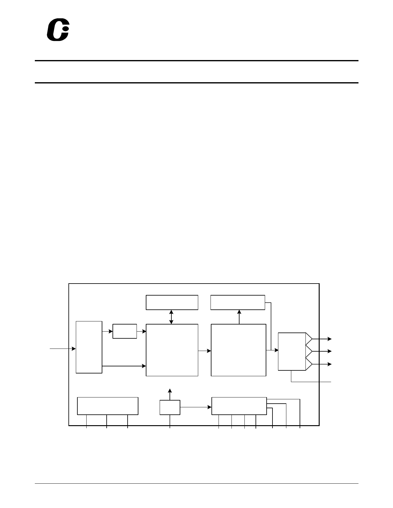
LINE
MEMORY
D[15:0]
PIXEL DATA
DIGITAL
INPUT
INTERFACE
RGB-YUV
CONVERTER
TRUE SCALE
SCALING & DEFLICKERING
ENGINE
YUV-RGB CONVERTER
NTSC/PAL
ENCODER
& FILTERS
TRIPLE
DAC
SYSTEM CLOCK
SERIAL CONTROL BLOCK
PLL
TIMING & SYNC GENERATOR
CLOCK
DATA
ADDR
XCLK
H V XI XO/FIN CSYNC P-OUT BCO
Figure 1: Functional Block Diagram
Y/R
C/G
CVBS/B
RSET
201-0000-069 Rev. 1.2, 9/1/2004
1
1 page 
CHRONTEL
CH7013B
4. DIGITAL VIDEO INTERFACE
The CH7013B digital video interface provides a flexible digital interface between a computer graphics controller
and the TV encoder IC, forming the ideal quality/cost configuration for performing the TV-output function. This
digital interface consists of up to 16 data signals and 4 control signals, all of which are subject to programmable
control through the CH7013B register set. This interface can be configured as 8, 12 or 16-bit inputs operating in
either multiplexed mode or 16-bit input operation in de-multiplexed mode. It will also accept either YCrCb or RGB
(15, 16 or 24-bit) data formats and will accept both non-interlaced and interlaced data formats. A summary of the
input data format modes is as follows:
Table 2. Input Data Formats
Bus
Width
16-bit
15-bit
16-bit
8-bit
8-bit
8-bit
8-bit
12-bit
12-bit
16-bit
Transfer Mode
Non-multiplexed
Non-multiplexed
Non-multiplexed
2X-multiplexed
2X-multiplexed
3X-multiplexed
2X-multiplexed
2X-multiplexed
2X-multiplexed
2X-multiplexed
Color Space and Depth
RGB 16-bit
RGB 15-bit
YCrCb (24-bit)
RGB 15-bit
RGB 16-bit
RGB 24-bit
YCrCb (24-bit)
RGB 24
RGB 24
RGB 24 (32)
Format Reference
5-6-5 each word
5-5-5 each word
CbY0,CrY1...(CCIR656 style)
5-5-5 over two bytes
5-6-5 over two bytes
8-8-8 over three bytes
Cb,Y0,Cr,Y1,(CCIR656 style)
8-8-8 over two words - ‘C’ version
8-8-8 over two words - ‘I’ version
8-8,8X over two words
The clock and timing signals used to latch and process the incoming pixel data is dependent upon the clock mode.
The CH7013B can operate in either master (the CH7013B generates a pixel frequency which is either returned as a
phase-aligned pixel clock or used directly to latch data), or slave mode (the graphics chip generates the pixel clock).
The pixel clock frequency will change depending upon the active image size (e.g., 640x480 or 800x600), the desired
output format (NTSC or PAL), and the amount of scaling desired. The pixel clock may be requested to be 1X, 2X, or
3X the pixel data rate (subject to a 100MHz frequency limitation). In the case of a 1X pixel clock the CH7013B will
automatically use both clock edges, if a multiplexed data format is selected.
Sync Signals: Horizontal and vertical sync signals will normally be supplied by the VGA controller, but may be
selected to be generated by the CH7013B. In the case of CCIR656 style input (IDF = 1 or 9), embedded sync may
also be used. (In each case, the period of the horizontal sync should be equal to the duration of the pixel clock, times
the first value of the (Total Pixels/Line x Total Lines/Frame) column of the (display Mode Register 00h
description). The leading edge of the horizontal sync is used to determine the start of each line. The Vertical sync
signal must be able to be set to the second value in the: (Total Pixels/Line x Total Lines/Frame) column of Table
17).
Master Clock Mode: The CH7013B generates a clock signal (output at the P-OUT pin) which will be used by the
VGA controller as a frequency reference. The VGA controller will then generate a clock signal which will be input
via the XCLK input. This incoming signal will be used to latch (and de-multiplex, if required) incoming data. The
XCLK input clock rate must match the input data rate, and the P-OUT clock can be requested to be 1X, 2X or 3X
the pixel data rate. As an alternative, the P-OUT clock signal can also be used as the input clock signal (connected
directly to the XCLK input) to latch the incoming data. If this mode is used, the incoming data must meet setup and
hold times with respect to the XCLK input (with the only internal adjustment being XCLK polarity).
Slave Clock Mode: The VGA controller will generate a clock which will be input to the XCLK pin (no clock signal
will be output on the P-OUT pin). This signal must match the input data rate, must occur at 1X, 2X or 3X the pixel
data rate, and will be used to latch (and de-multiplex if required) incoming data. Also, the graphics IC transmits
back to the TV encoder the horizontal and vertical timing signals, and pixel data, each of which must meet the
specified setup and hold times with respect to the pixel clock.
201-0000-069 Rev. 1.2, 9/1/2004
5
5 Page 
CHRONTEL
CH7013B
4.3 Functional Description
The CH7013B is a TV-output companion chip to graphics controllers providing digital output in either YUV or
RGB format. This solution involves both hardware and software elements which work together to produce an
optimum TV screen image based on the original computer generated pixel data. All essential circuitry for this
conversion are integrated on-chip. On-chip circuitry includes memory, memory control, scaling, PLL, DAC, filters,
and NTSC/PAL encoder. All internal signal processing, including NTSC/PAL encoding, is performed using digital
techniques to ensure that the high-quality video signals are not affected by drift issues associated with analog
components. No additional adjustment is required during manufacturing.
CH7013B is ideal for PC motherboards, web browsers, or VGA add-in boards where a minimum of discrete support
components (passive components, parallel resonance 14.31818 MHz crystal) are required for full operation.
4.3.1 Architectural Overview
The CH7013B is a complete TV output subsystem which uses both hardware and software elements to produce an
image on TV which is virtually identical to the image that would be displayed on a monitor. Simply creating a
compatible TV output from a VGA input involves a relatively straightforward process. This process includes a
standard conversion from RGB to YUV color space, converting from a non-interlaced to an interlaced frame
sequence, and encoding the pixel stream into NTSC or PAL compliant format. However, creating an optimum
computer-generated image on a TV screen involves a highly sophisticated process of scaling, deflickering, and
filtering. This results in a compatible TV output that displays a sharp and subtle image, of the right size, with
minimal artifacts from the conversion process.
As a key part of the overall system solution, the CH7013B software establishes the correct framework for the VGA
input signal to enable this process. Once the display is set to a supported resolution (either 640x480 or 800x600), the
CH7013B software may be invoked to establish the appropriate TV output display. The software then programs the
various timing parameters of the VGA controller to create an output signal that will be compatible with the chosen
resolution, operating mode, and TV format. Adjustments performed in software include pixel clock rates, total
pixels per line, and total lines per frame. By performing these adjustments in software, the CH7013B can render a
superior TV image without the added cost of a full frame buffer memory – normally used to implement features
such as scaling and full synchronization.
The CH7013B hardware accepts digital RGB or YCrCb inputs, which are latched in synchronization with the pixel
clock. These inputs are then color-space converted into YUV in 4-2-2 format and stored in a line buffer memory.
The stored pixels are fed into a block where scan-rate conversion, underscan scaling and 2-line, 3-line, 4-line and 5-
line vertical flicker filtering are performed. The scan-rate converter transforms the VGA horizontal scan-rate to
either NTSC or PAL scan rates; the vertical flicker filter eliminates flicker at the output while the underscan scaling
reduces the size of the displayed image to fit onto a TV screen. The resulting YUV signals are filtered through
digital filters to minimize aliasing problems. The digital encoder receives the filtered signals and transforms them to
composite and S-Video outputs, which are converted by the three 9-bit DACs into analog outputs.
In order to minimize the hazard of ESD, a set of protection diodes
MUST BE used for each DAC connecting to TV (Refer to AN-38 for details).
4.3.2 Color Burst Generation*
The CH7013B allows the sub-carrier frequency to be accurately generated from a 14.31818 MHz crystal oscillator,
leaving the sub-carrier frequency independent of the sampling rate. As a result, the CH7013B may be used with any
VGA chip (with an appropriate digital interface) since the CH7013B sub-carrier frequency can be generated without
being dependent on the precise pixel rates of VGA controllers. This feature is a significant benefit, since even a ±
0.01% sub-carrier frequency variation may be enough to cause some television monitors to lose color lock.
In addition, the CH7013B has the capability to genlock the color burst signal to the VGA horizontal sync frequency,
which enables a fully synchronous system between the graphics controller and the television. When genlocked, the
CH7013B can also stop “dot crawl” motion (for composite mode operation in NTSC modes) to eliminate the
annoyance of moving borders. Both of these features are under programmable control through the register set.
201-0000-069 Rev. 1.2, 9/1/2004
11
11 Page | ||
| Páginas | Total 30 Páginas | |
| PDF Descargar | [ Datasheet CH7013B.PDF ] | |
Hoja de datos destacado
| Número de pieza | Descripción | Fabricantes |
| CH7013A | Digital PC to TV Encoder | Chrontel |
| CH7013B | Digital PC to TV Encoder | Chrontel |
| Número de pieza | Descripción | Fabricantes |
| SLA6805M | High Voltage 3 phase Motor Driver IC. |
Sanken |
| SDC1742 | 12- and 14-Bit Hybrid Synchro / Resolver-to-Digital Converters. |
Analog Devices |
|
DataSheet.es es una pagina web que funciona como un repositorio de manuales o hoja de datos de muchos de los productos más populares, |
| DataSheet.es | 2020 | Privacy Policy | Contacto | Buscar |