|
|
|
PDF DS12887 Data sheet ( Hoja de datos )
| Número de pieza | DS12887 | |
| Descripción | Real Time Clock | |
| Fabricantes | Dallas | |
| Logotipo | ||
Hay una vista previa y un enlace de descarga de DS12887 (archivo pdf) en la parte inferior de esta página. Total 19 Páginas | ||
|
No Preview Available !
www.dalsemi.com
DS12887
Real Time Clock
FEATURES
§ Drop–in replacement for IBM AT computer
clock/calendar
§ Pin-compatible with the MC146818B and
DS1287
§ Totally nonvolatile with over 10 years of
operation in the absence of power
§ Self–contained subsystem includes lithium,
quartz, and support circuitry
§ Counts seconds, minutes, hours, days, day of
the week, date, month, and year with leap
year compensation valid up to 2100
§ Binary or BCD representation of time,
calendar, and alarm
§ 12– or 24–hour clock with AM and PM in
12–hour mode
§ Daylight Savings Time option
§ Selectable between Motorola and Intel bus
timing
§ Multiplex bus for pin efficiency
§ Interfaced with software as 128 RAM
locations
– 14 bytes of clock and control registers
– 114 bytes of general purpose RAM
§ Programmable square wave output signal
§ Bus–compatible interrupt signals ( IRQ )
§ Three interrupts are separately software–
maskable and testable
– Time–of–day alarm once/second to
once/day
– Periodic rates from 122 ms to 500 ms
– End of clock update cycle
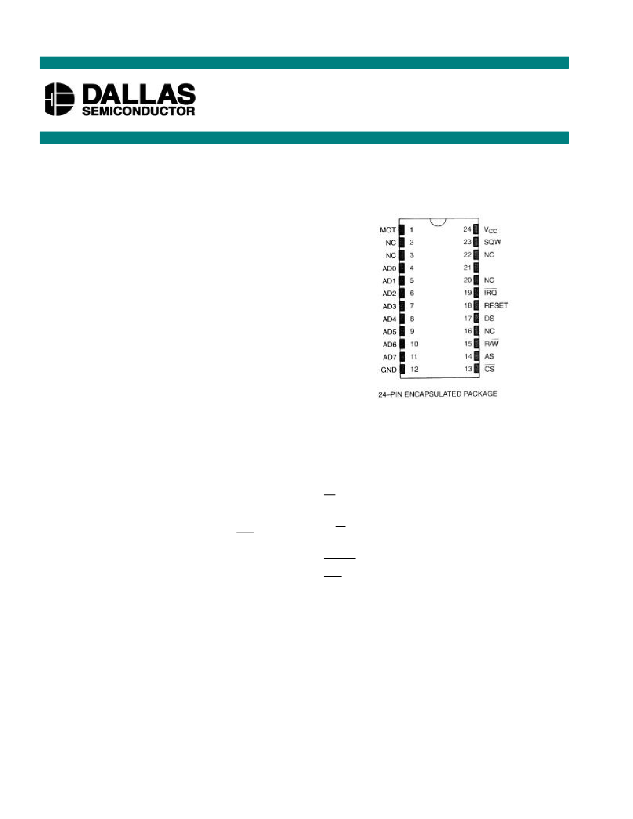
PIN ASSIGNMENT
NC
PIN DESCRIPTION
AD0–AD7 – Multiplexed Address/Data Bus
NC – No Connection
MOT
– Bus Type Selection
CS – Chip Select
AS – Address Strobe
R/ W – Read/Write Input
DS – Data Strobe
RESET
– Reset Input
IRQ
SQW
VCC
GND
– Interrupt Request Output
– Square Wave Output
– +5 Volt Supply
– Ground
DESCRIPTION
The DS12887 Real Time Clock plus RAM is designed to be a direct replacement for the DS1287. The
DS12887 is identical in form, fit, and function to the DS1287, and has an additional 64 bytes of general
purpose RAM. Access to this additional RAM space is determined by the logic level presented on AD6
during the address portion of an access cycle. A lithium energy source, quartz crystal, and write–
protection circuitry are contained within a 24–pin dual in-line package. As such, the DS12887 is a
complete subsystem replacing 16 components in a typical application. The functions include a nonvolatile
time–of–day clock, an alarm, a one-hundred–year calendar, programmable interrupt, square wave
1 of 19
110899
1 page 
A. Periodic Interrupt Enable (PEI) bit is cleared to 0.
B. Alarm Interrupt Enable (AIE) bit is cleared to 0.
C. Update Ended Interrupt Flag (UF) bit is cleared to 0.
D. Interrupt Request Status Flag (IRQF) bit is cleared to 0.
E. Periodic Interrupt Flag (PF) bit is cleared to 0.
F. The device is not accessible until RESET is returned high.
G. Alarm Interrupt Flag (AF) bit is cleared to 0.
H. IRQ pin is in the high impedance state.
I. Square Wave Output Enable ( SQWE ) bit is cleared to 0.
J. Update Ended Interrupt Enable (UIE) is cleared to 0.
DS12887
In a typical application RESET can be connected to VCC. This connection will allow the DS12887 to go in
and out of power fail without affecting any of the control registers.
ADDRESS MAP
The address map of the DS12887 is shown in Figure 2. The address map consists of 114 bytes of user
RAM, 10 bytes of RAM that contain the RTC time, calendar, and alarm data, and 4 bytes which are used
for control and status. All 128 bytes can be directly written or read except for the following:
1. Registers C and D are read–only.
2. Bit 7 of Register A is read–only.
3. The high order bit of the seconds byte is read–only.
The contents of four registers (A,B,C, and D) are described in the “Registers” section.
ADDRESS MAP DS12887 Figure 2
5 of 19
5 Page 
DS12887
DSE
The Daylight Savings Enable (DSE) bit is a read/write bit which enables two special updates when DSE
is set to 1. On the first Sunday in April the time increments from 1:59:59 AM to 3:00:00 AM. On the last
Sunday in October when the time first reaches 1:59:59 AM it changes to 1:00:00 AM. These special
updates do not occur when the DSE bit is a 0. This bit is not affected by internal functions or RESET .
REGISTER C
MSB
BIT 7
BIT 6
IRQF
PF
BIT 5
AF
BIT 4
UF
BIT 3
0
BIT 2
0
BIT 1
0
LSB
BIT 0
0
IRQF
The Interrupt Request Flag (IRQF) bit is set to a 1 when one or more of the following are true:
PF = PIE = 1
AF = AIE = 1
UF = UIE = 1
That is, IRQF = PF • PIE + AF • AIE + UF • UIE.
Any time the IRQF bit is a 1, the IRQ pin is driven low. All flag bits are cleared after Register C is read
by the program or when the RESET pin is low.
PF
The Periodic Interrupt Flag (PF) is a read–only bit which is set to a 1 when an edge is detected on the
selected tap of the divider chain. The RS3 through RS0 bits establish the periodic rate. PF is set to a 1
independent of the state of the PIE bit. When both PF and PIE are 1s, the IRQ signal is active and will set
the IRQF bit. The PF bit is cleared by a RESET or a software read of Register C.
AF
A 1 in the Alarm Interrupt Flag (AF) bit indicates that the current time has matched the alarm time. If the
AIE bit is also a 1, the IRQ pin will go low and a 1 will appear in the IRQF bit. A RESET or a read of
Register C will clear AF.
UF
The Update Ended Interrupt Flag (UF) bit is set after each update cycle. When the UIE bit is set to 1, the
one in UF causes the IRQF bit to be a 1, which will assert the IRQ pin. UF is cleared by reading Register
C or a RESET .
BIT 0 THROUGH BIT 3
These are unused bits of the status Register C. These bits always read 0 and cannot be written.
REGISTER D
MSB
BIT 7
BIT 6
VRT
0
BIT 5
0
BIT 4
0
BIT 3
0
11 of 19
BIT 2
0
BIT 1
0
LSB
BIT 0
0
11 Page | ||
| Páginas | Total 19 Páginas | |
| PDF Descargar | [ Datasheet DS12887.PDF ] | |
Hoja de datos destacado
| Número de pieza | Descripción | Fabricantes |
| DS12885 | (DS12xxx) Real Time Clock | Maxim Integrated Products |
| DS12885 | Real-Time Clock | Dallas Semiconductor |
| DS12885Q | Real-Time Clock | Dallas Semiconductor |
| DS12885T | Real-Time Clock | Dallas Semiconductor |
| Número de pieza | Descripción | Fabricantes |
| SLA6805M | High Voltage 3 phase Motor Driver IC. |
Sanken |
| SDC1742 | 12- and 14-Bit Hybrid Synchro / Resolver-to-Digital Converters. |
Analog Devices |
|
DataSheet.es es una pagina web que funciona como un repositorio de manuales o hoja de datos de muchos de los productos más populares, |
| DataSheet.es | 2020 | Privacy Policy | Contacto | Buscar |