|
|
|
PDF CA3060 Data sheet ( Hoja de datos )
| Número de pieza | CA3060 | |
| Descripción | 110kHz / Operational Transconductance Amplifier Array | |
| Fabricantes | Intersil | |
| Logotipo | ||
Hay una vista previa y un enlace de descarga de CA3060 (archivo pdf) en la parte inferior de esta página. Total 12 Páginas | ||
|
No Preview Available !
Semiconductor
CA3060January 1999
NO
Call
CRoeErnOCetrOBmaSMlaOAiMl:pLEpEcNlTeiDcnEaEtaPtDipoRpRnO@sEDP1hUL-aC8Ar0rTCi0sE-.4cM4o2Em-N7T747Transconducta1n1c0ekHAzm, pOlpifieerratAiorrnaayl
Features
Description
[ /Title
(CA30
60)
/Sub-
ject
(110k
Hz,
Opera-
tional
Transc
onduc-
tance
Ampli-
fier
Array)
/Autho
r ()
/Key-
words
(Har-
ris
Semi-
con-
ductor,
triple,
transco
nduc-
tance
ampli-
fier,
low
power
op
amp,
• Low Power Consumption as Low as 100mW Per
Amplifier
• Independent Biasing for Each Amplifier
• High Forward Transconductance
• Programmable Range of Input Characteristics
• Low Input Bias and Input Offset Current
• High Input and Output Impedance
• No Effect on Device Under Output Short-Circuit
Conditions
• Zener Diode Bias Regulator
Applications
• For Low Power Conventional Operational Amplifier
Applications
• Active Filters
• Comparators
• Gyrators
• Mixers
• Modulators
• Multiplexers
• Multipliers
• Strobing and Gating Functions
• Sample and Hold Functions
The CA3060 monolithic integrated circuit consists of an array of
three independent Operational Transconductance Amplifiers
(see Note). This type of amplifier has the generic characteris-
tics of an operational voltage amplifier with the exception that
the forward gain characteristic is best described by transcon-
ductance rather than voltage gain (open-loop voltage gain is the
product of the transconductance and the load resistance,
gMRL). When operated into a suitable load resistor and with
provisions for feedback, these amplifiers are well suited for a
wide variety of operational-amplifier and related applications. In
addition, the extremely high output impedance makes these
types particularly well suited for service in active filters.
The three amplifiers in the CA3060 are identical push-pull
Class A types which can be independently biased to achieve a
wide range of characteristics for specific application. The elec-
trical characteristics of each amplifier are a function of the
amplifier bias current (IABC). This feature offers the system
designer maximum flexibility with regard to output current capa-
bility, power consumption, slew rate, input resistance, input bias
current, and input offset current. The linear variation of the
parameters with respect to bias and the ability to maintain a
constant DC level between input and output of each amplifier
also makes the CA3060 suitable for a variety of nonlinear appli-
cations such as mixers, multipliers, and modulators.
In addition, the CA3060 incorporates a unique Zener diode
regulator system that permits current regulation below sup-
ply voltages normally associated with such systems.
NOTE: Generic applications of the OTA are described in AN-6668.
For improved input operating ranges, refer to CA3080 and CA3280
data sheets (File Nos. 475 and 1174) and application notes AN6668
and AN6818.
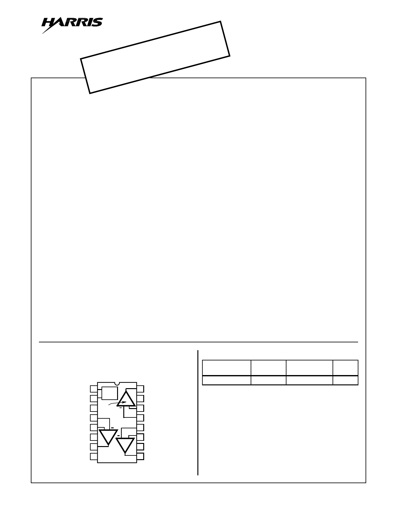
Pinout
CA3060
(PDIP)
TOP VIEW
REGULATOR OUT 1
REGULATOR IN 2
BIAS
REG.
V+ 3 AMP 1
INV. INPUT NO. 3 4
NON-INV. INPUT NO. 3 5
BIAS NO. 3 6
OUTPUT NO. 3 7
AMP
3
AMP
2
V- 8
16 OUTPUT NO. 1
15 BIAS NO. 1
14 NON-INV. INPUT NO. 1
13 INV. INPUT NO. 1
12 INV. INPUT NO. 2
11 NON-INV. INPUT NO. 2
10 BIAS NO. 2
9 OUTPUT NO. 2
Part Number Information
PART NUMBER
CA3060E
TEMP.
RANGE (oC)
PACKAGE
-40 to 85 16 Ld PDIP
PKG.
NO.
E16.3
CAUTION: These devices are sensitive to electrostatic discharge. Users should follow proper IC Handling Procedures.
Copyright © Harris Corporation 1999
3-1
File Number 537.4
1 page 
CA3060
Typical Performance Curves (Continued)
14
13
12
6
5
4
3
-3
-4
-5
-6
-12
-13
-14
-15
1
VOM+ (MIN)
±15V SUPPLY
VOM+ (MIN)
±6V SUPPLY
VOM- (MIN)
±6V SUPPLY
VOM+ (TYP)
±15V SUPPLY
VOM+ (TYP)
±6V SUPPLY
VOM- (MIN)
±15V SUPPLY
VOM- (TYP)
±15V SUPPLY
VOM- (TYP)
±6V SUPPLY
10 100
AMPLIFIER BIAS CURRENT (µA)
1000
FIGURE 7. PEAK OUTPUT VOLTAGE vs AMPLIFIER BIAS
CURRENT
10,000
1000
TA = 25oC
SUPPLY VOLTAGE:
VS = ±6
VS = ±15
MAXIMUM
100
TYPICAL
10
1 10 100 1000
AMPLIFIER BIAS CURRENT (µA)
FIGURE 8. AMPLIFIER SUPPLY CURRENT (EACH AMPLIFIER)
vs AMPLIFIER BIAS CURRENT
1000
100
IABC = 100µA
IABC = 30µA
IABC = 10µA
IABC = 3µA
10
IABC = 1µA
SUPPLY VOLTAGE: V+ = 6V, V- = -6V
V+ = 15V, V- = -15V
1
-75 -50
-25 0 25 50 75
TEMPERATURE (oC)
100
125
FIGURE 9. AMPLIFIER SUPPLY CURRENT (EACH AMPLIFIER)
vs TEMPERATURE
800
SUPPLY VOLTAGE: VVS = ±6
VS = ±15
750
700
650
600
550
500
1
10 100
AMPLIFIER BIAS CURRENT (µA)
1000
FIGURE 10. AMPLIFIER BIAS VOLTAGE vs AMPLIFIER BIAS
CURRENT
1000
100
TA = 25oC, f = 1kHz
SUPPLY VOLTAGE: VS = ±6
VS = ±15
TYPICAL
10 MINIMUM
1
1000
TA = 25oC, f = 1kHz
SUPPLY VOLTAGE: VS = ±6
VS = ±15
100
IABC = 30µA
10
IABC = 100µA
IABC = 10µA
1 10 100 1000
AMPLIFIER BIAS CURRENT (µA)
FIGURE 11. FORWARD TRANSCONDUCTANCE vs AMPLIFIER
BIAS CURRENT
IABC = 1µA
1
-50 -25 0 25 50 75 100 125
TEMPERATURE (oC)
FIGURE 12. FORWARD TRANSCONDUCTANCE vs
TEMPERATURE
3-5
5 Page 
CA3060
decreased to maintain the same value of source current.
The low cost dual gate protected MOSFET, 40841 type, may
be used when operating at the low supply voltage.
The phase compensation network consists of a single 390Ω
resistor and a 1000pF capacitor, located at the interface of the
CA3060 output and the MOSFET gate. The bandwidth of the
system is 1.5MHz and the slew rate is 0.3V/µs. The system
slew rate is directly proportional to the value of the phase
compensation capacitor. Thus, with higher gain settings
where lower values of phase compensation capacitors are
possible, the slew rate is proportionally increased.
Non-Linear Applications
AM Modulator (Two Quadrant Multiplier)
Figure 26 shows Amplifier 3 of the CA3060 used in an AM
modulator or two quadrant multiplier circuit. When modula-
tion is applied to the amplifier bias input, Terminal B, and the
carrier frequency to the differential input, Terminal A, the
waveform, shown in Figure 26 is obtained. Figure 26 is a
result of adjusting the input offset control to balance the
circuit so that no modulation can occur at the output without
a carrier input. The linearity of the modulator is indicated by
the solid trace of the superimposed modulating frequency.
The maximum depth of modulation is determined by the ratio
of the peak input modulating voltage to V-.
The two quadrant multiplier characteristic of this modulator is
easily seen if modulation and carrier are reversed as shown in
Figure 26. The polarity of the output must follow that of the dif-
ferential input; therefore, the output is positive only during, the
positive half cycle of the modulation and negative only in the
second half cycle. Note, that both the input and output signals
are referenced to ground. The output signal is zero when
either the differential input or IABC are zero.
Four Quadrant Multiplier
The CA3060 is also useful as a four quadrant multiplier. A
block diagram of such a multiplier, utilizing Amplifiers 1, 2
and 3 is shown in Figure 27 and a typical circuit is shown in
Figure 28. The multiplier consists of a single CA3060 and,
as in the two quadrant multiplier, exhibits no level shift
between input and output. In Figure 27, Amplifier 1 is
connected as an inverting amplifier for the X-input signal.
The output current of Amplifier 1 is calculated as follows:
IO(1) = [-VX] [g21(1)]
EQ. 1
Amplifier 2 is a non-inverting amplifier so that
IO(2) = [+VX] [g21(2)]
EQ. 2
Because the amplifier output impedances are high, the load
current is the sum of the two output currents, for an output
voltage
VO = VXRL [g21(2) - g21(1)]
EQ. 3
The transconductance is approximately proportional to the
amplifier bias current; therefore, by varying the bias current
the g21 is also controlled. Amplifier 2 bias current is propor-
tional to the Y-input signal and is expressed as
IABC(2) ≈ (---V-------R)----+-1----V----Y--
EQ. 4
Hence,
g21(2) ≈ k [(V-) + VY]
EQ. 5
Bias for Amplifier 1 is derived from the output of Amplifier 3
which is connected as a unity gain inverting amplifier.
IABC(1), therefore, varies inversely with VY. And by the same
reasoning as above
g21(1) ≈ k [(V-) - VY]
EQ. 6
Combining Equations 3, 5 and 6 yields:
VO ≈ VX x k x RL {[(V-) + VY] - [(V-) - VY]} or
VO ≈ 2kRLVXVY
+6V
CARRIER
TERM.
A
10kΩ
1kΩ
3
4-
AMP 3
5+
1kΩ
8
1MΩ
6
-6V
V+
MODULATION
V-
100kΩ
1MΩ
TERM.
B
10kΩ
MODULATED
OUTPUT
7
100kΩ
FIGURE 26. TWO QUADRANT MULTIPLIER CIRCUIT USING THE CA3060 WITH ASSOCIATED WAVEFORMS
3-11
11 Page | ||
| Páginas | Total 12 Páginas | |
| PDF Descargar | [ Datasheet CA3060.PDF ] | |
Hoja de datos destacado
| Número de pieza | Descripción | Fabricantes |
| CA3060 | 110kHz / Operational Transconductance Amplifier Array | Intersil |
| CA3062 | Photo Detector & Power Amplifier | ETC |
| CA3064 | TV Automatic Fine Tuning Circuit | RCA Solid State |
| CA3065 | IF Amplifier-Limiter / FM Detector / Audio Driver | RCA Solid State |
| Número de pieza | Descripción | Fabricantes |
| SLA6805M | High Voltage 3 phase Motor Driver IC. |
Sanken |
| SDC1742 | 12- and 14-Bit Hybrid Synchro / Resolver-to-Digital Converters. |
Analog Devices |
|
DataSheet.es es una pagina web que funciona como un repositorio de manuales o hoja de datos de muchos de los productos más populares, |
| DataSheet.es | 2020 | Privacy Policy | Contacto | Buscar |