|
|
|
PDF ADN2819 Data sheet ( Hoja de datos )
| Número de pieza | ADN2819 | |
| Descripción | Multirate to 2.7 Gb/s Clock and Data Recovery IC with Integrated Limiting Amp | |
| Fabricantes | Analog Devices | |
| Logotipo | ||
Hay una vista previa y un enlace de descarga de ADN2819 (archivo pdf) en la parte inferior de esta página. Total 24 Páginas | ||
|
No Preview Available !
Multirate to 2.7 Gb/s Clock and Data
Recovery IC with Integrated Limiting Amp
ADN2819
FEATURES
PRODUCT DESCRIPTION
Meets SONET requirements for jitter
transfer/generation/tolerance
Quantizer sensitivity: 4 mV typical
Adjustable slice level: ±100 mV
1.9 GHz minimum bandwidth
Patented clock recovery architecture
Loss of signal detect range: 3 mV to 15 mV
Single reference clock frequency for all rates, including
15/14 (7%) wrapper rate
Choice of 19.44 MHz, 38.88 MHz, 77.76 MHz, or 155.52 MHz
REFCLK
LVPECL/LVDS/LVCMOS/LVTTL compatible inputs
(LVPECL/LVDS only at 155.52 MHz)
19.44 MHz oscillator on-chip to be used with external crystal
The ADN2819 provides the receiver functions of quantization,
signal level detect, and clock and data recovery at rates of OC-3,
OC-12, OC-48, Gigabit Ethernet, and 15/14 FEC rates. All
SONET jitter requirements are met, including jitter transfer,
jitter generation, and jitter tolerance. All specifications are
quoted for –40°C to +85°C ambient temperature, unless
otherwise noted.
The device is intended for WDM system applications, and can
be used with either an external reference clock or an on-chip
oscillator with external crystal. Both native rates and 15/14 rate
digital wrappers are supported by the ADN2819, without any
change of reference clock.
Loss of lock indicator
This device, together with a PIN diode and a TIA preamplifier,
Loopback mode for high speed test data
can implement a highly integrated, low cost, low power, fiber
Output squelch and bypass features
optic receiver.
Single-supply operation: 3.3 V
Low power: 540 mW typical
7 mm × 7 mm 48-lead LFCSP
APPLICATIONS
SONET OC-3/-12/-48, SDH STM-1/-4/-16, GbE and 15/14
FEC rates
WDM transponders
Regenerators/repeaters
The receiver front end signal detect circuit indicates when the
input signal level has fallen below a user-adjustable threshold.
The signal detect circuit has hysteresis to prevent chatter at the
output.
The ADN2819 is available in a compact 7 mm × 7 mm, 48-lead
chip scale package.
Test equipment
Backplane applications
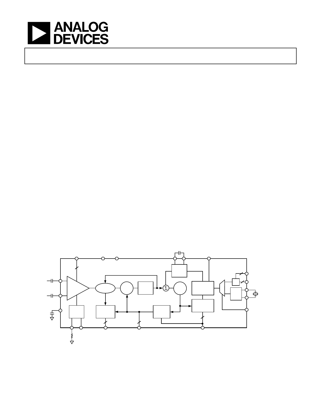
FUNCTIONAL BLOCK DIAGRAM
SLICEP/N
VCC VEE
CF1 CF2
LOL
2 ADN2819
PIN
QUANTIZER
NIN
PHASE
SHIFTER
PHASE
DET.
LOOP
FILTER
LOOP
FILTER
VCO
FREQUENCY
LOCK
DETECTOR
VREF
LEVEL
DETECT
THRADJ SDOUT
DATA
RETIMING
2
DATAOUTP/N
DIVIDER
1/2/4/16
2
CLKOUTP/N
FRACTIONAL
DIVIDER
3
SEL[0..2]
2
2
/n
XTAL
OSC
REFSEL[0..1]
REFCLKP/N
XO1
XO2
REFSEL
Figure 1.
Rev. B
Information furnished by Analog Devices is believed to be accurate and reliable.
However, no responsibility is assumed by Analog Devices for its use, nor for any
infringements of patents or other rights of third parties that may result from its use.
Specifications subject to change without notice. No license is granted by implication
or otherwise under any patent or patent rights of Analog Devices. Trademarks and
registered trademarks are the property of their respective owners.
One Technology Way, P.O. Box 9106, Norwood, MA 02062-9106, U.S.A.
Tel: 781.329.4700
www.analog.com
Fax: 781.326.8703 © 2004 Analog Devices, Inc. All rights reserved.
1 page 
Parameter
Setup Time
Hold Time
REFCLK DC INPUT CHARACTERISTICS
Input Voltage Range
Peak-to-Peak Differential Input
Common-Mode Level
TEST DATA DC INPUT CHARACTERISTICS4 (TDINP/N)
Peak-to-Peak Differential Input Voltage
LVTTL DC INPUT CHARACTERISTICS
Input High Voltage
Input Low Voltage
Input Current
Input Current (SEL0 and SEL1 Only)5
LVTTL DC OUTPUT CHARACTERISTICS
Output High Voltage
Output Low Voltage
Conditions
TS (See Figure 3)
OC-48
GbE
OC-12
OC-3
TH (See Figure 3)
OC-48
GbE
OC-12
OC-3
@ REFCLKP or REFCLKN
DC-coupled, single-ended
CML inputs
VIH
VIL
VIN = 0.4 V or VIN = 2.4 V
VIN = 0.4 V or VIN = 2.4 V
VOH, IOH = –2.0 mA
VOL, IOL = +2.0 mA
ADN2819
Min Typ Max Unit
140
350
750
3145
ps
ps
ps
ps
150
350
750
3150
ps
ps
ps
ps
0 VCC V
100 mV
VCC/2
V
0.8 V
2.0 V
–5
–5
0.8 V
+5 µA
+50 µA
2.4 V
0.4 V
1 PIN and NIN should be differentially driven, ac-coupled for optimum sensitivity.
2 PWD measurement made on quantizer outputs in bypass mode.
3 Jitter tolerance measurements are equipment limited.
4 TDINP/N are CML inputs. If the drivers to the TDINP/N inputs are anything other than CML, they must be ac-coupled.
5 SEL0 and SEL1 have internal pull-down resistors, causing higher IIH.
Rev. B | Page 5 of 24
5 Page 
ADN2819
OC3_JIT_TOLERANCE
GBE_JIT_TOLERANCE
OC3_JIT_TRANSFER
GBE_JIT_TRANSFER
0.5
OC12_JIT_TOLERANCE
OC48_JIT_TOLERANCE
OC12_JIT_TRANSFER
OC48_JIT_TRANSFER
0
–0.5
–1.0
–1.5
–2.0
–2.5
–3.0
–3.5
–4.0
–4.5
–5.0
–5.5
–6.0
–6.5
–7.0
–7.5
–8.0
–8.5
–9.0
–9.5
–10.0
1k
10k 100k 1M
FREQUENCY (Hz)
Figure 14. Jitter Transfer and Jitter Tracking BW
10M
100M
Table 4. Jitter Transfer and Tolerance: SONET Spec vs. ADN2819
Jitter Transfer
ADN2819 Implementation Mask Corner
Rate SONET Spec (fC) (kHz)
Margin
Frequency
OC-48 2 MHz
590 3.4
1 MHz
OC-12 500 kHz
140 3.6
250 kHz
OC-3 130 kHz
48 2.7
65 kHz
ADN2819
4.8 MHz
4.8 MHz
600 kHz
Jitter Tolerance
SONET Spec ADN2819
(UI p-p)
(UI p-p)
0.15 1.0
0.15 1.0
0.15 1.0
Implementation
Margin1
6.67
6.67
6.67
1 Jitter tolerance measurements limited by test equipment capabilities.
Rev. B | Page 11 of 24
11 Page | ||
| Páginas | Total 24 Páginas | |
| PDF Descargar | [ Datasheet ADN2819.PDF ] | |
Hoja de datos destacado
| Número de pieza | Descripción | Fabricantes |
| ADN2811 | OC-48/OC-48 FEC Clock and Data Recovery IC | Analog Devices |
| ADN2812 | Continuous Rate 12.3 Mb/s to 2.7 Gb/s Clock and Data Recovery IC with Integrated Limiting Amp | Analog Devices |
| ADN2813 | Clock and Data Recovery IC | Analog Devices |
| ADN2814 | Continuous Rate 12.3 Mb/s to 675 Mb/s Clock and Data Recovery IC | Analog Devices |
| Número de pieza | Descripción | Fabricantes |
| SLA6805M | High Voltage 3 phase Motor Driver IC. |
Sanken |
| SDC1742 | 12- and 14-Bit Hybrid Synchro / Resolver-to-Digital Converters. |
Analog Devices |
|
DataSheet.es es una pagina web que funciona como un repositorio de manuales o hoja de datos de muchos de los productos más populares, |
| DataSheet.es | 2020 | Privacy Policy | Contacto | Buscar |