|
|
|
PDF WM2613 Data sheet ( Hoja de datos )
| Número de pieza | WM2613 | |
| Descripción | Byte-wide Parallel Input/ 12-bit Voltage Output DAC | |
| Fabricantes | Wolfson Microelectronics plc | |
| Logotipo | ||
Hay una vista previa y un enlace de descarga de WM2613 (archivo pdf) en la parte inferior de esta página. Total 11 Páginas | ||
|
No Preview Available !
WM2613
Byte-wide Parallel Input, 12-bit Voltage Output DAC
Production Data, June 1999, Rev 1.0
FEATURES
• Dual 12-bit voltage output DAC
• Dual supply 2.7V to 5.5V operation
• DNL ±0.4 LSB, INL ±1.5 LSB
• Programmable settling time 1µs or 3µs typical
• 8-bit micro controller compatible interface
• Power down mode (10nA)
APPLICATIONS
• Battery powered test instruments
• Digital offset and gain adjustment
• Battery operated/remote industrial controls
• Machine and motion control devices
• Wireless telephone and communication systems
• Speech synthesis
• Arbitrary waveform generation
ORDERING INFORMATION
DESCRIPTION
The WM2613 is a 12-bit voltage output, resistor string, digital-to-
analogue converter. The DAC can be powered down under
software or hardware control, reducing power consumption to
10nA.
The device has an 8-bit microcontroller compatible parallel
interface. The eight data LSBs, the four data MSBs, and the three
control bits are written using three different addresses.
Excellent performance is delivered with a typical DNL of 0.4 LSBs.
The output stage is buffered by a x2 gain near rail-to-rail amplifier,
which features a Class A output stage (slow mode, class AB). The
settling time of the DAC is software programmable to allow the
designer to optimize speed versus power dissipation.
The device is available in a 20-pin TSSOP package. Commercial
temperature (0° to 70°C) and Industrial temperature (-40° to 85°C)
variants are supported.
DEVICE
WM2613CDT
WM2613IDT
TEMP. RANGE
0° to 70°C
-40° to 85°C
PACKAGE
20-pin TSSOP
20-pin TSSOP
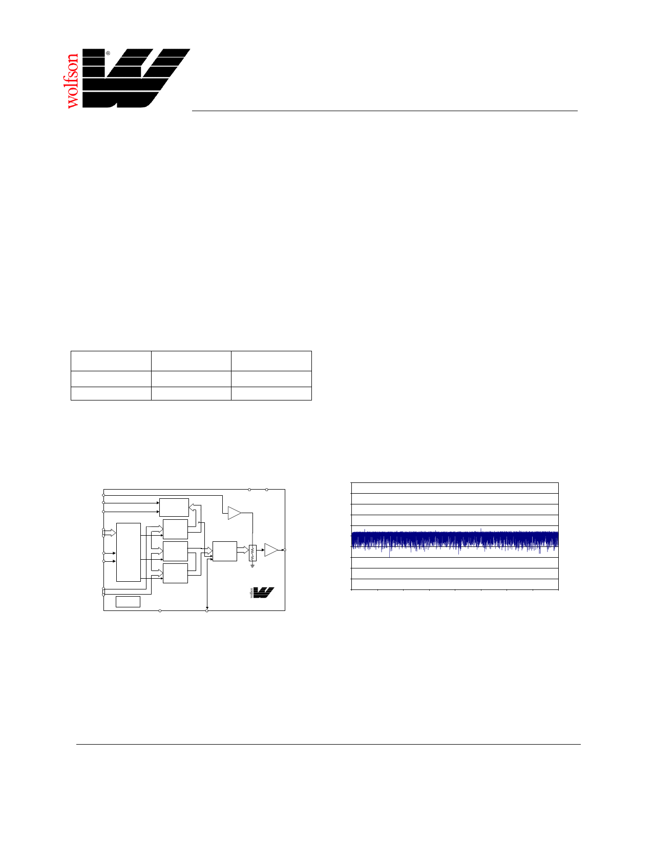
BLOCK DIAGRAM
REFIN(12)
SPD (9)
NPD (15)
A[0-1] (8,7)
NCS (18)
NWE (17)
PARALLEL
INTERFACE
AND
CONTROL
LOGIC
D[0-7]
(19,20, 1-6)
POWER-ON
RESET
POWERDOWN/
SPEED
CONTROL
3-BIT
CONTROL
LATCH
4-BIT DAC
MSW
HOLDING
LATCH
8-BIT DAC
LSW
HOLDING
LATCH
DV DD
(10)
AVDD
(11)
REFERENCE
INPUT BUFFER
X1
12-BIT DAC
LATCH
DAC
OUTPUT
BUFFER
X2
(13) OUT
(14)
GND
(16)
NLDAC
WM2613
TYPICAL PERFORMANCE
1
0.8
0.6
0.4
0.2
0
-0.2
-0.4
-0.6
-0.8
-1
0
AVDD = DVDD = 5V, VREF = 2.048V, Speed = Fast mode, Load = 10k/100pF
512
1024
1536
2048
2559
3071
DIGITAL CODE
3583
4095
WOLFSON MICROELECTRONICS LTD
Lutton Court, Bernard Terrace, Edinburgh, EH8 9NX, UK
Tel: +44 (0) 131 667 9386
Fax: +44 (0) 131 667 5176
Email: [email protected]
http://www.wolfson.co.uk
Production Data Datasheets contain final
specifications current on publication date.
Supply of products conforms to Wolfson
Microelectronics’ Terms and conditions.
Master rev 1.0.doc June 17, 1999 14:12
©1999 Wolfson Microelectronics Ltd.
1 page 
Production Data
WM2613
Test Conditions:
RL = 10kΩ, CL = 100pF. AVDD = DVDD = 5V ± 10%, VREF = 2.048V and AVDD = DVDD = 3V ± 10%, VREF = 1.024V over
recommended operating free-air temperature range (unless noted otherwise)
PARAMETER
Reference
SYMBOL
TEST
CONDITIONS
MIN TYP
MAX
UNIT
Reference input resistance
RREFIN
10 MΩ
Reference input capacitance
CREFIN
5 pF
Reference feedthrough
Reference input bandwidth
Digital Inputs
VREF = 1VPP at 1kHz
+ 1.024V d.c., DAC code 0
VREF = 0.2VPP + 1.024V d.c.
DAC code 2048
Slow
Fast
-60
1
1.6
dB
MHz
MHz
High level input current
IIH Input voltage = DVDD
1 µA
Low level input current
IIL Input voltage = 0V
-1 µA
Input capacitance
CI
8 pF
Notes:
1. Integral non-linearity (INL) is the maximum deviation of the output from the line between zero and full scale excluding the
effects of zero code and full scale errors).
2. Differential non-linearity (DNL) is the difference between the measured and ideal 1LSB amplitude change
of any adjacent two codes. A guarantee of monotonicity means the output voltage changes in the same
direction (or remains constant) as a change in digital input code.
3. Zero code error is the voltage output when the DAC input code is zero.
4. Gain error is the deviation from the ideal full scale output excluding the effects of zero code error.
5. Power supply rejection ratio is measured by varying AVDD from 4.5V to 5.5V and measuring the
proportion of this signal imposed on the zero code error and the gain error.
6. Zero code error and Gain error temperature coefficients are normalised to full scale voltage.
7. Output load regulation is the difference between the output voltage at full scale with a 10kΩ load and 2kΩ
load. It is expressed as a percentage of the full scale output voltage with a 10kΩ load.
8. IDD is measured while continuously writing code 2048 to the DAC. For VIH < DVDD - 0.7V and VIL > 0.7V supply current
will increase.
9. Typical supply current in power down mode is 10nA. Production test limits are wider for speed of test.
10. Slew rate results are for the lower value of the rising and falling edge slew rates.
11. Settling time is the time taken for the signal to settle to within 0.5LSB of the final measured value for both rising and
falling edges. Limits are ensured by design and characterisation, but are not production tested
12. SNR, SNRD, THD and SPFDR are measured on a synthesised sinewave at frequency fOUT generated with
a sampling frequency fS.
WOLFSON MICROELECTRONICS LTD
Production Data Rev 1.0 June 1999
5
5 Page 
Production Data
PACKAGE DIMENSIONS
DT: 20 PIN TSSOP (6.5 x 4.4 x 1.0 mm)
b
20
e
11
WM2613
DM008.C
E1 E
1 10
D
GAUGE
PLANE
θ
A A2 A1
0.05 C
-C-
SEATING PLANE
cL
Symbols
A
A1
A2
b
c
D
e
E
E1
L
θ
Dimensions
(mm)
MIN
NOM
MAX
----- ----- 1.20
0.05 ----- 0.15
0.80 1.00 1.05
0.19 ----- 0.30
0.09 ----- 0.20
6.40 6.50 6.60
0.65 BSC
6.4 BSC
4.30 4.40 4.50
0.45
0o
0.60
-----
0.75
8o
REF:
JEDEC.95, MO-153
NOTES:
A. ALL LINEAR DIMENSIONS ARE IN MILLIMETERS.
B. THIS DRAWING IS SUBJECT TO CHANGE WITHOUT NOTICE.
C. BODY DIMENSIONS DO NOT INCLUDE MOLD FLASH OR PROTRUSION, NOT TO EXCEED 0.25MM.
D. MEETS JEDEC.95 MO-153, VARIATION = AC. REFER TO THIS SPECIFICATION FOR FURTHER DETAILS.
0.25
WOLFSON MICROELECTRONICS LTD
Production Data Rev 1.0 June 1999
11
11 Page | ||
| Páginas | Total 11 Páginas | |
| PDF Descargar | [ Datasheet WM2613.PDF ] | |
Hoja de datos destacado
| Número de pieza | Descripción | Fabricantes |
| WM2610 | Octal 12-bit/ Serial Input/ Voltage Output DAC with Power Down | Wolfson Microelectronics plc |
| WM2613 | Byte-wide Parallel Input/ 12-bit Voltage Output DAC | Wolfson Microelectronics plc |
| WM2614 | Quad 12-bit Serial Input Voltage Output DAC | Wolfson Microelectronics plc |
| WM2616 | 12-bit Serial Input Voltage Output DAC | Wolfson Microelectronics plc |
| Número de pieza | Descripción | Fabricantes |
| SLA6805M | High Voltage 3 phase Motor Driver IC. |
Sanken |
| SDC1742 | 12- and 14-Bit Hybrid Synchro / Resolver-to-Digital Converters. |
Analog Devices |
|
DataSheet.es es una pagina web que funciona como un repositorio de manuales o hoja de datos de muchos de los productos más populares, |
| DataSheet.es | 2020 | Privacy Policy | Contacto | Buscar |