|
|
|
PDF W199 Data sheet ( Hoja de datos )
| Número de pieza | W199 | |
| Descripción | Spread Spectrum FTG for VIA Apollo Pro-133 | |
| Fabricantes | Cypress Semiconductor | |
| Logotipo | ||
Hay una vista previa y un enlace de descarga de W199 (archivo pdf) en la parte inferior de esta página. Total 14 Páginas | ||
|
No Preview Available !
PRELIMINARY
W199
Spread Spectrum FTG for VIA Apollo Pro-133
Features
• Maximized EMI suppression using Cypress’s Spread
Spectrum Technology
• Single-chip system frequency synthesizer for VIA
Apollo Pro-133
• Two copies of CPU output
• Six copies of PCI output
• One 48-MHz output for USB
• One 24-MHz output for SIO
• Two buffered reference outputs
• One IOAPIC output
• 13 SDRAM outputs provide support for 3 DIMMs
• Supports frequencies up to 150 MHz
• I2C™ interface for programming
• Power management control inputs
• Available in 48-pin SSOP
Key Specifications
CPU Cycle-to-Cycle Jitter: ......................................... 250 ps
CPU to CPU Output Skew: ........................................ 175 ps
PCI to PCI Output Skew: ............................................ 500 ps
VDDQ3: .................................................................... 3.3V±5%
VDDQ2: .................................................................... 2.5V±5%
SDRAMIN to SDRAM0:11 Delay: ..........................3.7 ns typ.
SDRAM0:11 (leads) to SDRAM_F Skew: ..............0.4 ns typ.
Table 1. Mode Input Table
Mode
0
1
Pin 2
PCI_STOP#
REF0
Table 2. Pin Selectable Frequency
Input Address
CPU_F,
FS3 FS2 FS1 FS0 CPU1 (MHz)
111 1
133.3
111 0
124
110 1
150
110 0
140
101 1
105
101 0
110
100 1
115
100 0
120
011 1
100
011 0
133.3
010 1
112
010 0
103
001 1
66.8
001 0
83.3
000 1
75
000 0
124
PCI_F, 1:5
(MHz)
33.3 (CPU/4)
31 (CPU/4)
37.5 (CPU/4)
35 (CPU/4)
35 (CPU/3)
36.7 (CPU/3)
38.3 (CPU/3)
40 (CPU/3)
33.3 (CPU/3)
44.43 (CPU/3)
37.3 (CPU/3)
34.3 (CPU/3)
33.4 (CPU/2)
41.7 (CPU/2)
37.5 (CPU/2)
41.3 (CPU/3)
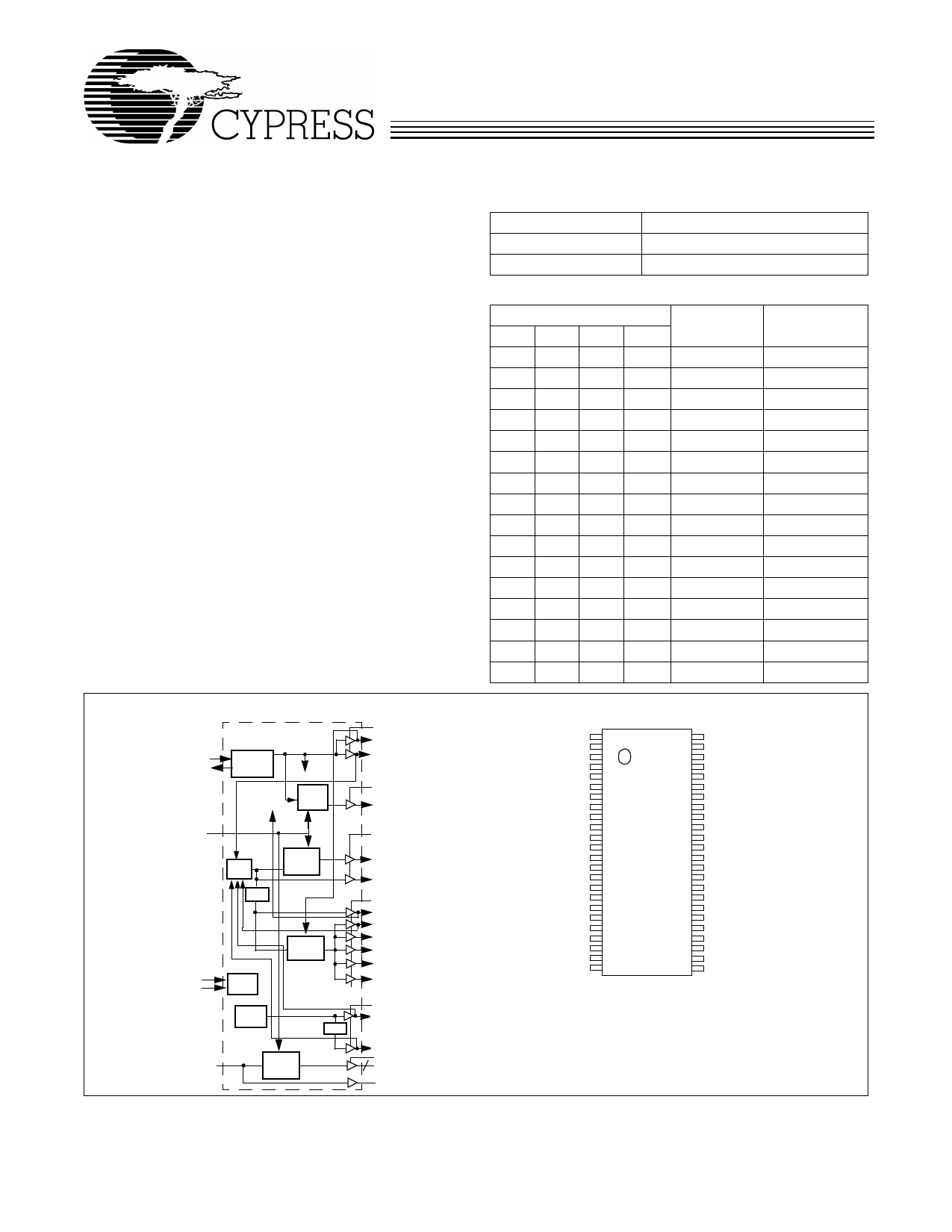
Logic Block Diagram
X1 XTAL
X2 OSC
PLL Ref Freq
I/O Pin
Control
Stop
Clock
Control
CLK_STOP#
PLL 1
Stop
Clock
Control
÷2,3,4
SDATA
SCLK
I2C
Logic
PLL2
Stop
Clock
Control
÷2
VDDQ3
REF0/(PCI_STOP#)
REF1/FS2
VDDQ2
IOAPIC
VDDQ2
CPU1
CPU_F
VDDQ3
PCI_F/MODE
PCI1/FS3
PCI2
PCI3
PCI4
PCI5
VDDQ3
48MHz/FS0
Pin Configuration[1]
VDDQ3
REF0/(PCI_STOP#)
GND
X1
X2
VDDQ3
PCI_F/MODE
PCI1/FS3
GND
PCI2
PCI3
PCI4
PCI5
VDDQ3
SDRAMIN
GND
SDRAM11
SDRAM10
VDDQ3
SDRAM9
SDRAM8
GND
{I2C SDATA
SCLK
1
2
3
4
5
6
7
8
9
10
11
12
13
14
15
16
17
18
19
20
21
22
23
24
48 VDDQ2
47 IOAPIC
46 REF1/FS2*
45 GND
44 CPU_F
43 CPU1
42 VDDQ2
41 CLK_STOP#
40 SDRAM_F
39 GND
38 SDRAM0
37 SDRAM1
36 VDDQ3
35 SDRAM2
34 SDRAM3
33 GND
32 SDRAM4
31 SDRAM5
30 VDDQ3
29 SDRAM6
28 SDRAM7
27 VDDQ3
26 48MHz/FS0*
25 24MHz/FS1*
SDRAMIN
Stop
Clock
Control
24MHz/FS1
VDDQ3
SDRAM0:11
12
SDRAM_F
I2C is a trademark of Philips Corporation.
Note:
1. Internal pull-up resistors should not be relied upon for setting I/O pins HIGH. Pin function with parentheses determined by MODE pin resistor strapping.
Unlike other I/O pins, input FS3 has an internal pull-down resistor.
Cypress Semiconductor Corporation • 3901 North First Street • San Jose • CA 95134 • 408-943-2600
October 19, 1999, rev. **
1 page 
PRELIMINARY
W199
Serial Data Interface
The W199 features a two-pin, serial data interface that can be
used to configure internal register settings that control partic-
ular device functions. Upon power-up, the W199 initializes with
default register settings, therefore the use of this serial data
interface is optional. The serial interface is write-only (to the
clock chip) and is the dedicated function of device pins SDATA
and SCLOCK. In motherboard applications, SDATA and
SCLOCK are typically driven by two logic outputs of the
chipset. Clock device register changes are normally made
upon system initialization, if any are required. The interface
can also be used during system operation for power manage-
ment functions. Table 3 summarizes the control functions of
the serial data interface.
Operation
Data is written to the W199 in eleven bytes of eight bits each.
Bytes are written in the order shown in Table 4.
Table 3. Serial Data Interface Control Functions Summary
Control Function
Clock Output Disable
CPU Clock Frequency
Selection
Spread Spectrum
Enabling
Output Three-state
(Reserved)
Description
Any individual clock output(s) can be disabled.
Disabled outputs are actively held LOW.
Provides CPU/PCI frequency selections through
software. Frequency is changed in a smooth and
controlled fashion.
Enables or disables spread spectrum clocking.
Common Application
Unused outputs are disabled to reduce EMI
and system power. Examples are clock
outputs to unused PCI slots.
For alternate microprocessors and power
management options. Smooth frequency
transition allows CPU frequency change
under normal system operation.
For EMI reduction.
Puts clock output into a high-impedance state.
Reserved function for future device revision or
production device testing.
Production PCB testing.
No user application. Register bit must be
written as 0.
Table 4. Byte Writing Sequence
Byte
Sequence
1
Byte Name
Slave Address
Bit Sequence
11010010
2 Command Code Don’t Care
3 Byte Count
Don’t Care
4 Data Byte 0
5 Data Byte 1
6 Data Byte 2
7 Data Byte 3
8 Data Byte 4
9 Data Byte 5
10 Data Byte 6
11 Data Byte 7
Refer to Table 5
Byte Description
Commands the W199 to accept the bits in Data Bytes 0–6 for internal
register configuration. Since other devices may exist on the same com-
mon serial data bus, it is necessary to have a specific slave address for
each potential receiver. The slave receiver address for the W199 is
11010010. Register setting will not be made if the Slave Address is not
correct (or is for an alternate slave receiver).
Unused by the W199, therefore bit values are ignored (“don’t care”).
This byte must be included in the data write sequence to maintain
proper byte allocation. The Command Code Byte is part of the standard
serial communication protocol and may be used when writing to anoth-
er addressed slave receiver on the serial data bus.
Unused by the W199, therefore bit values are ignored (“don’t care”).
This byte must be included in the data write sequence to maintain
proper byte allocation. The Byte Count Byte is part of the standard
serial communication protocol and may be used when writing to anoth-
er addressed slave receiver on the serial data bus.
The data bits in Data Bytes 0–7 set internal W199 registers that control
device operation. The data bits are only accepted when the Address
Byte bit sequence is 11010010, as noted above. For description of bit
control functions, refer to Table 5, Data Byte Serial Configuration Map.
5
5 Page 
PRELIMINARY
W199
SDRAM Clock Outputs, SDRAM, SDRAM0:11 (Lump Capacitance Test Load = 30 pF) (continued)
PCI Clock Outputs, PCI_F and PCI1:5 (Lump Capacitance Test Load = 30 pF)
Parameter
Description
Test Condition/Comments
tP Period
Measured on rising edge at 1.5V
tH High Time
Duration of clock cycle above 2.4V
tL Low Time
Duration of clock cycle below 0.4V
tR Output Rise Edge Rate Measured from 0.4V to 2.4V
tF Output Fall Edge Rate Measured from 2.4V to 0.4V
tD Duty Cycle
Measured on rising and falling edge at 1.5V
tJC
Jitter, Cycle-to-Cycle
Measured on rising edge at 1.5V. Maximum
difference of cycle time between two adja-
cent cycles.
tSK Output Skew
Measured on rising edge at 1.5V
tO CPU to PCI Clock Skew Covers all CPU/PCI outputs. Measured on
rising edge at 1.5V. CPU leads PCI output.
fST Frequency Stabilization Assumes full supply voltage reached within
from Power-up (cold start) 1 ms from power-up. Short cycles exist pri-
or to frequency stabilization.
Zo AC Output Impedance Average value during switching transition.
Used for determining series termination
value.
Min.
30
12.0
12.0
1
1
45
1.5
Typ.
30
Max.
4
4
55
250
500
4
3
Unit
ns
ns
ns
V/ns
V/ns
%
ps
ps
ns
ms
Ω
IOAPIC Clock Output (Lump Capacitance Test Load = 20 pF)
Parameter
f
tR
tF
tD
fST
Zo
Description
Test Condition/Comments
Frequency, Actual
Frequency generated by crystal oscillator
Output Rise Edge Rate Measured from 0.4V to 2.0V
Output Fall Edge Rate Measured from 2.0V to 0.4V
Duty Cycle
Measured on rising and falling edge at 1.25V
Frequency Stabilization Assumes full supply voltage reached within
from Power-up (cold start) 1 ms from power-up. Short cycles exist prior
to frequency stabilization.
AC Output Impedance
Average value during switching transition.
Used for determining series termination value.
CPU = 66.6/100 MHz
Min. Typ. Max.
14.31818
14
14
45 55
1.5
15
Unit
MHz
V/ns
V/ns
%
ms
Ω
11
11 Page | ||
| Páginas | Total 14 Páginas | |
| PDF Descargar | [ Datasheet W199.PDF ] | |
Hoja de datos destacado
| Número de pieza | Descripción | Fabricantes |
| W191 | Skew Controlled SDRAM Buffer | SpectraLinear |
| W1934S | Color Monitor | LG |
| W194 | Frequency Multiplier and Zero Delay Buffer | Cypress Semiconductor |
| W1942S | LCD User Guide | LG |
| Número de pieza | Descripción | Fabricantes |
| SLA6805M | High Voltage 3 phase Motor Driver IC. |
Sanken |
| SDC1742 | 12- and 14-Bit Hybrid Synchro / Resolver-to-Digital Converters. |
Analog Devices |
|
DataSheet.es es una pagina web que funciona como un repositorio de manuales o hoja de datos de muchos de los productos más populares, |
| DataSheet.es | 2020 | Privacy Policy | Contacto | Buscar |