|
|
|
PDF W161 Data sheet ( Hoja de datos )
| Número de pieza | W161 | |
| Descripción | 133-MHz Spread Spectrum FTG for Pentium II Platforms | |
| Fabricantes | Cypress Semiconductor | |
| Logotipo | ||
Hay una vista previa y un enlace de descarga de W161 (archivo pdf) en la parte inferior de esta página. Total 9 Páginas | ||
|
No Preview Available !
PRELIMINARY
W161
133-MHz Spread Spectrum FTG for Pentium® II Platforms
Features
• Maximized EMI Suppression using Cypress’s Spread
Spectrum Technology
• Three copies of CPU outputs at 100 or 133 MHz
• Three copies of 66-MHz output at 3.3V
• Ten copies of PCI clocks at 33 MHz, 3.3V
• Two copies of 14.318-MHz reference output at 3.3V
• One copy of 48-MHz USB clock
• One copy of CPU-divide-by-2 output as reference input
to Direct Rambus™ Clock Generator (Cypress W134)
• Available in 48-pin SSOP (300 mils)
Key Specifications
Supply Voltages: ...................................... VDDQ2 = 2.5V±5%
VDDQ3 = 3.3V±5%
CPU, CPUdiv2 Output Jitter:....................................... 250 ps
CPU, CPUdiv2 Output Skew: ...................................... 175 ps
IOAPIC, 3V66 Output Skew: ....................................... 250 ps
PCI0:9 Output Skew: .................................................. 500 ps
Duty Cycle: ................................................................... 45/55
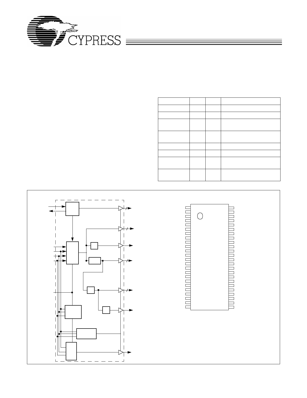
Block Diagram
X1 XTAL
X2 OSC
2
REF_[0:1]
3
CPU_[0:2]
SPREAD#
SEL0
SEL1
SEL133/100#
PLL 1
÷2
÷2/÷1.5
CPUdiv2
3
3V66_[0:2]
PWRDWN#
÷2
Power
Down
Logic
÷2
Three-state
Logic
9
PCI_[0:9]
IOAPIC
Spread Spectrum Modulation:..................................... –0.5%
CPU to 3V66 Output Offset: ............. 0.0–1.5 ns (CPU leads)
3V66 to PCI Output Offset:.............. 1.5–3.0 ns (3V66 leads)
CPU to IOAPIC Output Offset: ......... 1.5–4.0 ns (CPU leads)
Table 1. Pin Selectable Frequency
SEL133/100# SEL1 SEL0
Function
0 0 0 All outputs Three-State
0 0 1 (Reserved)
0 1 0 Active 100-MHz, 48-MHz
PLL inactive
0 1 1 Active 100-MHz, 48-MHz
PLL active
1 0 0 Test Mode
1 0 1 (Reserved)
1 1 0 Active 133-MHz, 48-MHz
PLL inactive
1 1 1 Active 133-MHz, 48-MHz
PLL active
Pin Configuration[1]
REF0
REF1
VDDQ3
X1
X2
GND
PCI0
PCI1
VDDQ3
PCI2
PCI3
PCI4
PCI5
GND
PCI6
PCI7
VDDQ3
PCI8
PCI9
GND
3V66_0
3V66_1
3V66_2
VDDQ3
1
2
3
4
5
6
7
8
9
10
11
12
13
14
15
16
17
18
19
20
21
22
23
24
48 GND
47 VDDQ2
46 IOAPIC
45 GND
44 VDDQ2
43 CPUdiv2
42 GND
41 VDDQ2
40 CPU2
39 GND
38 VDDQ2
37 CPU1
36 CPU0
35 GND
34 VDDQ3
33 GND
32 PWRDWN#*
31 SPREAD#*
30 SEL1*
29 SEL0*
28 VDDQ3
27 48MHz
26 GND
25 SEL133/100#
Note:
1. Internal 250-kΩ pull-up resistors present on inputs marked with *.
Design should not rely solely on internal pull-up resistor to set I/O
pins HIGH.
PLL2
48MHz
Pentium is a registered trademark of Intel Corporation. Direct Rambus is a trademark of Rambus, Inc.
Cypress Semiconductor Corporation • 3901 North First Street • San Jose • CA 95134 • 408-943-2600
October 13, 1999, rev. **
1 page 
PRELIMINARY
W161
DC Electrical Characteristics: TA = 0°C to +70°C, VDDQ3 = 3.3V±5%, VDDQ2 = 2.5V±5% (continued)
Parameter
Description
Test Condition
Min.
Typ.
Max.
Crystal Oscillator
VTH X1 Input threshold Voltage[4]
CLOAD
Load Capacitance, Imposed on
External Crystal[5]
CIN,X1
X1 Input Capacitance[6]
Pin Capacitance/Inductance
Pin X2 unconnected
1.65
18
28
CIN
COUT
LIN
Input Pin Capacitance
Output Pin Capacitance
Input Pin Inductance
Except X1 and X2
5
6
7
Unit
V
pF
pF
pF
pF
nH
3.3V AC Electrical Characteristics
TA = 0°C to +70°C, VDDQ3 = 3.3V±5%,VDDQ2 = 2.5V± 5%, fXTL = 14.31818 MHz
Spread Spectrum function turned off
AC clock parameters are tested and guaranteed over stated operating conditions using the stated lump capacitive load at the
clock output.[7]
3V66 Clock Outputs, 3V66_0:3 (Lump Capacitance Test Load = 30 pF)
Parameter
Description
Test Condition/Comments
Min. Typ. Max. Unit
f Frequency
Note 8
66.6 MHz
tR Output Rise Edge Rate Measured from 0.4V to 2.4V
1
tF
Output Fall Edge Rate
Measured from 2.4V to 0.4V
1
tD Duty Cycle
Measured on rising and falling edge at 1.5V 45
fST Frequency Stabilization Assumes full supply voltage reached within
from Power-up (cold start) 1 ms from power-up. Short cycles exist prior
to frequency stabilization.
4 V/ns
4 V/ns
55 %
3 ms
Zo
AC Output Impedance
Average value during switching transition.
Used for determining series termination
value.
15
Ω
Notes:
4. X1 input threshold voltage (typical) is VDD/2.
5. The W161 contains an internal crystal load capacitor between pin X1 and ground and another between pin X2 and ground. Total load placed on crystal is 18 pF;
this includes typical stray capacitance of short PCB traces to crystal.
6. X1 input capacitance is applicable when driving X1 with an external clock source (X2 is left unconnected).
7. Period, jitter, offset, and skew measured on rising edge at 1.5V.
8. 3V66 is CPU/2 for CPU =133 MHz and (2 x CPU)/3 for CPU = 100 MHz.
5
5 Page | ||
| Páginas | Total 9 Páginas | |
| PDF Descargar | [ Datasheet W161.PDF ] | |
Hoja de datos destacado
| Número de pieza | Descripción | Fabricantes |
| W160A | 160 Lead Cerquad | National Semiconductor |
| W161 | 133-MHz Spread Spectrum FTG for Pentium II Platforms | Cypress Semiconductor |
| W162 | Spread Aware/ Zero Delay Buffer | Cypress Semiconductor |
| W163 | Spread Aware/ Zero Delay Buffer | Cypress Semiconductor |
| Número de pieza | Descripción | Fabricantes |
| SLA6805M | High Voltage 3 phase Motor Driver IC. |
Sanken |
| SDC1742 | 12- and 14-Bit Hybrid Synchro / Resolver-to-Digital Converters. |
Analog Devices |
|
DataSheet.es es una pagina web que funciona como un repositorio de manuales o hoja de datos de muchos de los productos más populares, |
| DataSheet.es | 2020 | Privacy Policy | Contacto | Buscar |