No Preview Available !

PCF8574; PCF8574A
Remote 8-bit I/O expander for I2C-bus with interrupt
Rev. 5 — 27 May 2013
Product data sheet
1. General description
The PCF8574/74A provides general-purpose remote I/O expansion via the two-wire
bidirectional I2C-bus (serial clock (SCL), serial data (SDA)).
The devices consist of eight quasi-bidirectional ports, 100 kHz I2C-bus interface, three
hardware address inputs and interrupt output operating between 2.5 V and 6 V. The
quasi-bidirectional port can be independently assigned as an input to monitor interrupt
status or keypads, or as an output to activate indicator devices such as LEDs. System
master can read from the input port or write to the output port through a single register.
The low current consumption of 2.5 A (typical, static) is great for mobile applications and
the latched output ports directly drive LEDs.
The PCF8574 and PCF8574A are identical, except for the different fixed portion of the
slave address. The three hardware address pins allow eight of each device to be on the
same I2C-bus, so there can be up to 16 of these I/O expanders PCF8574/74A together on
the same I2C-bus, supporting up to 128 I/Os (for example, 128 LEDs).
The active LOW open-drain interrupt output (INT) can be connected to the interrupt logic
of the microcontroller and is activated when any input state differs from its corresponding
input port register state. It is used to indicate to the microcontroller that an input state has
changed and the device needs to be interrogated without the microcontroller continuously
polling the input register via the I2C-bus.
The internal Power-On Reset (POR) initializes the I/Os as inputs with a weak internal
pull-up 100 A current source.
2. Features and benefits
I2C-bus to parallel port expander
100 kHz I2C-bus interface (Standard-mode I2C-bus)
Operating supply voltage 2.5 V to 6 V with non-overvoltage tolerant I/O held to VDD
with 100 A current source
8-bit remote I/O pins that default to inputs at power-up
Latched outputs directly drive LEDs
Total package sink capability of 80 mA
Active LOW open-drain interrupt output
Eight programmable slave addresses using three address pins
Low standby current (2.5 A typical)
40 C to +85 C operation
ESD protection exceeds 2000 V HBM per JESD22-A114 and 1000 V CDM per
JESD22-C101
1 page


NXP Semiconductors
PCF8574; PCF8574A
Remote 8-bit I/O expander for I2C-bus with interrupt
7. Functional description
Refer to Figure 1 “Block diagram”.
7.1 Device address
Following a START condition, the bus master must send the address of the slave it is
accessing and the operation it wants to perform (read or write). The address format of the
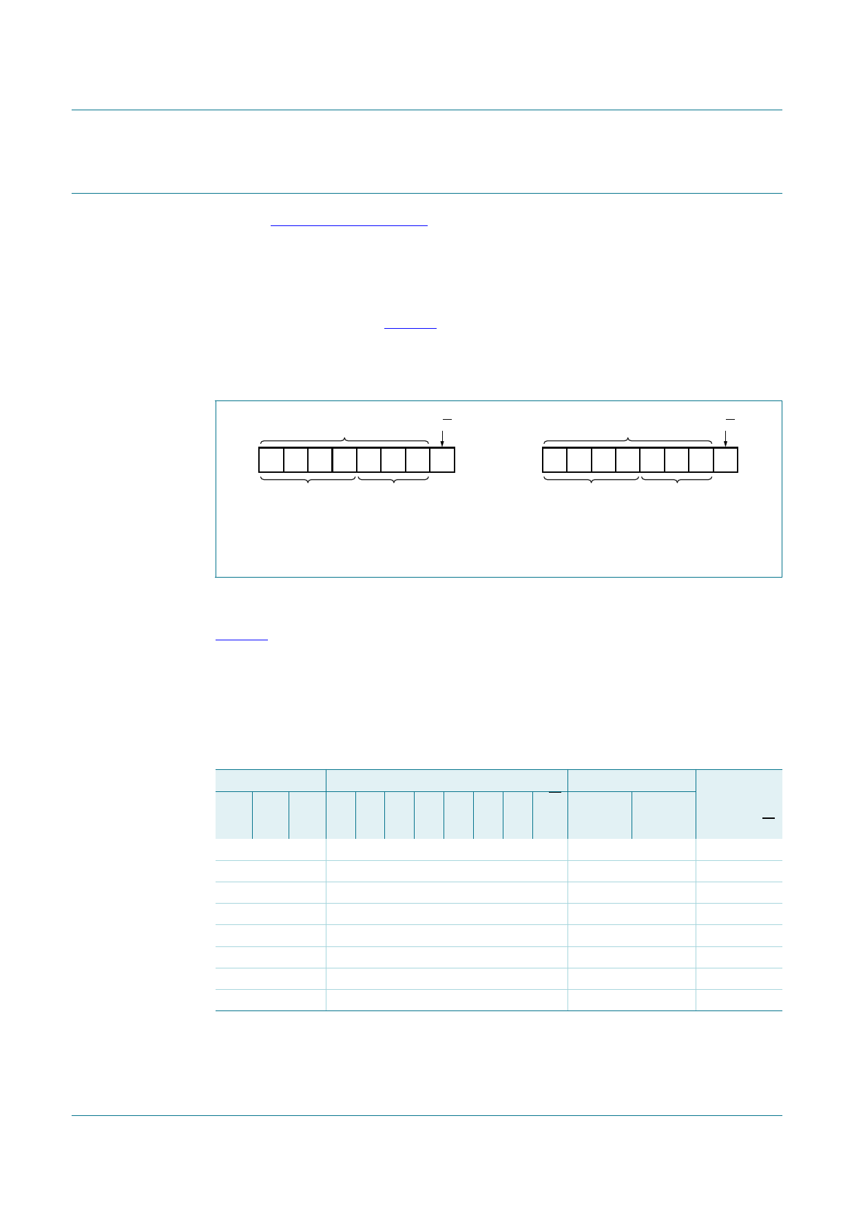
PCF8574/74A is shown in Figure 6. Slave address pins A2, A1 and A0 are held HIGH or
LOW to choose one of eight slave addresses. To conserve power, no internal pull-up
resistors are incorporated on A2, A1 or A0, so they must be externally held HIGH or LOW.
The address pins (A2, A1, A0) can connect to VDD or VSS directly or through resistors.
slave address
R/W
slave address
R/W
0 1 0 0 A2 A1 A0 0
0 1 1 1 A2 A1 A0 0
fixed
hardware
selectable
002aad628
fixed
hardware
selectable
002aad629
a. PCF8574
b. PCF8574A
Fig 6. PCF8574 and PCF8574A slave addresses
The last bit of the first byte defines the operation to be performed. When set to logic 1 a
read is selected, while a logic 0 selects a write operation (write operation is shown in
Figure 6).
7.1.1 Address maps
The PCF8574 and PCF8574A are functionally the same, but have a different fixed portion
(A6 to A3) of the slave address. This allows eight of the PCF8574 and eight of the
PCF8574A to be on the same I2C-bus without address conflict.
Table 4. PCF8574 address map
Pin connectivity
Address of PCF8574
Address byte value
7-bit
A2 A1 A0 A6 A5 A4 A3 A2 A1 A0 R/W Write
Read hexadecimal
address
without R/W
VSS VSS VSS 0 1 0 0 0 0 0 -
40h
41h
20h
VSS VSS VDD 0 1 0 0 0 0 1 -
42h
43h
21h
VSS VDD VSS 0 1 0 0 0 1 0 -
44h
45h
22h
VSS VDD VDD 0 1 0 0 0 1 1 -
46h
47h
23h
VDD VSS VSS 0 1 0 0 1 0 0 -
48h
49h
24h
VDD VSS VDD 0 1 0 0 1 0 1 -
4Ah
4Bh
25h
VDD VDD VSS 0 1 0 0 1 1 0 -
4Ch
4Dh
26h
VDD VDD VDD 0 1 0 0 1 1 1 -
4Eh
4Fh
27h
PCF8574_PCF8574A
Product data sheet
All information provided in this document is subject to legal disclaimers.
Rev. 5 — 27 May 2013
© NXP B.V. 2013. All rights reserved.
5 of 33
5 Page


NXP Semiconductors
PCF8574; PCF8574A
Remote 8-bit I/O expander for I2C-bus with interrupt
9. Characteristics of the I2C-bus
The I2C-bus is for 2-way, 2-wire communication between different ICs or modules. The
two wires are a serial data line (SDA) and a serial clock line (SCL). Both lines must be
connected to a positive supply via a pull-up resistor when connected to the output stages
of a device. Data transfer may be initiated only when the bus is not busy.
9.1 Bit transfer
One data bit is transferred during each clock pulse. The data on the SDA line must remain
stable during the HIGH period of the clock pulse as changes in the data line at this time
will be interpreted as control signals (see Figure 11).
SDA
SCL
Fig 11. Bit transfer
data line
stable;
data valid
change
of data
allowed
mba607
9.1.1 START and STOP conditions
Both data and clock lines remain HIGH when the bus is not busy. A HIGH-to-LOW
transition of the data line while the clock is HIGH is defined as the START condition (S). A
LOW-to-HIGH transition of the data line while the clock is HIGH is defined as the STOP
condition (P) (see Figure 12).
SDA
SCL
S
START condition
Fig 12. Definition of START and STOP conditions
P
STOP condition
mba608
9.2 System configuration
A device generating a message is a ‘transmitter’; a device receiving is the ‘receiver’. The
device that controls the message is the ‘master’ and the devices which are controlled by
the master are the ‘slaves’ (see Figure 13).
PCF8574_PCF8574A
Product data sheet
All information provided in this document is subject to legal disclaimers.
Rev. 5 — 27 May 2013
© NXP B.V. 2013. All rights reserved.
11 of 33
11 Page
| 


