|
|
|
PDF PC87366 Data sheet ( Hoja de datos )
| Número de pieza | PC87366 | |
| Descripción | 128-Pin LPC SuperI/O with System Hardware Monitoring/ MIDI and Game Ports | |
| Fabricantes | National Semiconductor | |
| Logotipo | ||
Hay una vista previa y un enlace de descarga de PC87366 (archivo pdf) en la parte inferior de esta página. Total 30 Páginas | ||
|
No Preview Available !
PRELIMINARY
January 11, 1999
PC87366
128-Pin LPC SuperI/O with System Hardware Monitoring,
MIDI and Game Ports
General Description
The PC87366, a member of National Semiconductor’s 128-pin
LPC SuperI/O family, combines National’s System Hardware
Monitoring capability with a Musical Instrument Digital Interface
(MIDI) Port and game port inputs for up to two joysticks. The
PC87366 is PC99 and ACPI compliant, and offers a single-
chip solution to the most commonly used PC I/O peripherals.
System Hardware Monitoring provides minimum power con-
sumption and maximum operating efficiency within the system
environment. It integrates National’s diode-based or thermistor-
based Temperature Sensor (TMS) with National’s Voltage Lev-
el Monitor (VLM) for full, PC system thermal control. The
PC87366 monitors system voltages using 8-bit Analog to Dig-
ital (A/D) conversion with seven analog input channels and four
internal measuring points.
The PC87366 also incorporates: Fan Speed Control and
Monitor (FSCM) for three fans, extended wake-up support
for a wide range of wake-up events, system design protection
features, a Floppy Disk Controller (FDC), a Keyboard and
Mouse Controller (KBC), a full IEEE 1284 Parallel Port, two
enhanced Serial Ports (UARTs), one with Infrared (IR) sup-
port, ACCESS.bus® Interface (ACB), System Wake-Up
Control (SWC), General-Purpose Input/Output (GPIO) sup-
port for 40 ports, Interrupt Serializer for Parallel IRQs and an
enhanced WATCHDOG™ timer (WDT).
Outstanding Features
q System Hardware Monitoring including:
— Diode-based or thermistor-based Temperature Sen-
sor (TMS)
— Voltage Level Monitor (VLM) with VID inputs
q MIDI interface compatible with MPU-401 UART mode
q Game port inputs for up to two joysticks
q Extended Wake-Up support, including legacy/ACPI
power button support, direct power supply control in
response to wake-up events, power-fail recovery
q Protection features, including chassis intrusion detection,
GPIO lock and pin configuration lock
q Fan Speed Control and Monitor for three fans
q Serial IRQ support (15 options)
q Interrupt Serializer (11 Parallel IRQs to Serial IRQ)
q Bus interface, based on Intel’s LPC Interface Specifi-
cation Revision 1.0, September 29th, 1997
q ACCESS.bus interface, SMBus physical layer compatible
q 40 GPIO Ports (29 standard, including 15 with Assert
IRQ/SMI/PWUREQs interrupts; 11 VSB-powered)
q Blinking LEDs
q 128-pin PQFP Package
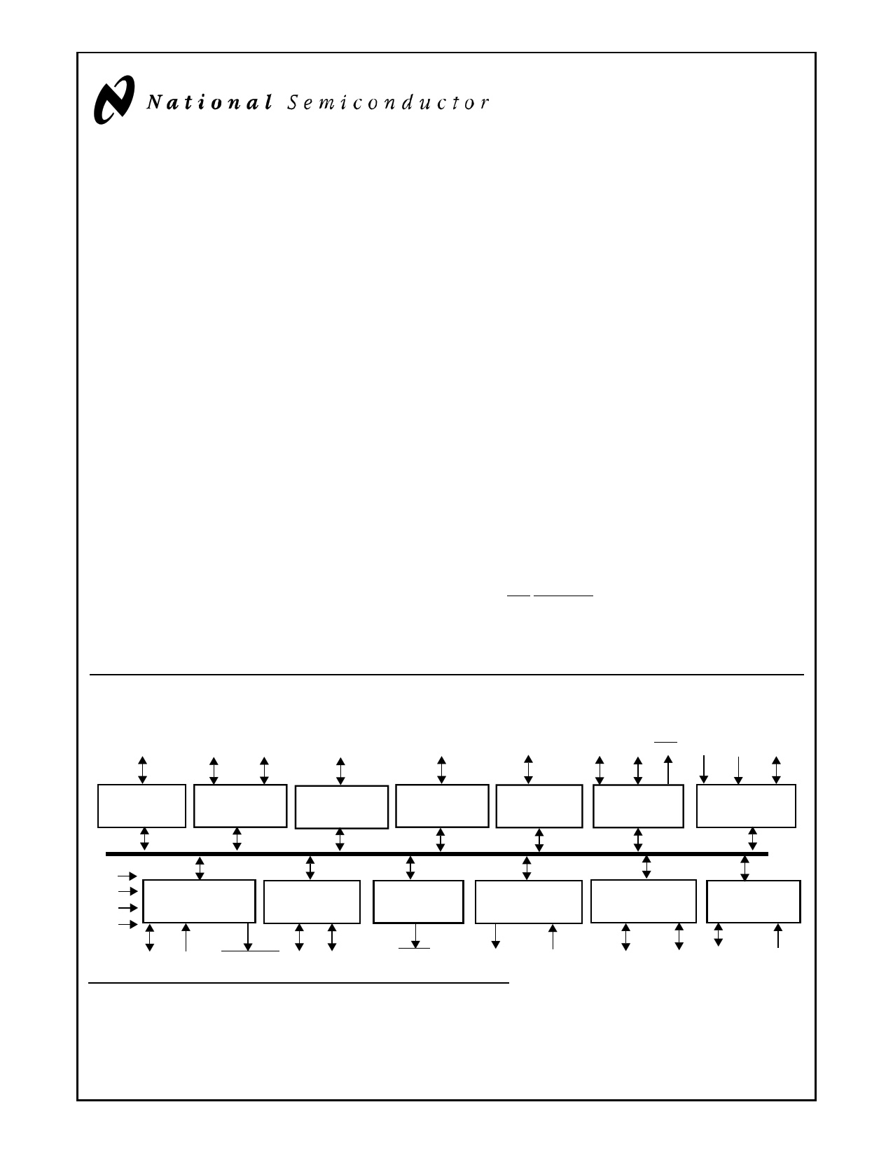
Block Diagram
Serial
Serial Infrared
Interface Interface Interface
I/O
Ports
Floppy Drive Parallel Port LPC Serial Analog
Diode
Interface
Interface Interface IRQ SMI Inputs VREF Interface
Serial Port 1
Serial Port 2
with IR
GPIO Ports
Floppy Disk IEEE 1284
Controller Parallel Port
Bus
Interface
System
Hardware
Monitoring
AV DD
VDD
VBdAT
VSB
System Wake-Up ACCESS.bus
Control
Interface
Power Wake-Up PWUREQ SCL SDA
Control Events
WATCHDOG
Fan Speed
Keyboard &
MIDI &
Timer
Control & Monitor Mouse Controller Game Ports
WDO
3 Control 3 Monitor Keyboard & Ports MIDI Game
Outputs Inputs Mouse I/F
Interface Inputs
ACCESS.bus® is a registered trademark of Digital Equipment Corporation.
I2C® is a registered trademark of Philips Corporation.
IBM®, MicroChannel®, PC-AT® and PS/2® are registered trademarks of International Business Machines Corporation.
Microsoft® and Windows® are registered trademarks of Microsoft Corporation.
TRI-STATE® is a registered trademark of National Semiconductor Corporation.
WATCHDOG‰ is a trademark of National Semiconductor Corporation.
SMBus® is a registered trademark of Intel Corporation.
© 1999 National Semiconductor Corporation
www.national.com
1 page 
Table of Contents
Datasheet Revision Record
............................................................................................................ 4
........................................................................................................................................................................... 4
1.0 Signal/Pin Connection and Description
1.1 CONNECTION DIAGRAM ......................................................................................................... 16
1.2 BUFFER TYPES AND SIGNAL/PIN DIRECTORY .................................................................... 17
1.3 PIN MULTIPLEXING ................................................................................................................. 22
1.4 DETAILED SIGNAL/PIN DESCRIPTIONS ................................................................................ 24
1.4.1 ACCESS.bus Interface (ACB) .................................................................................... 24
1.4.2 Bus Interface ............................................................................................................... 24
1.4.3 Clock ............................................................................................................................ 24
1.4.4 Fan Speed Control and Monitor (FSCM) ..................................................................... 24
1.4.5 Floppy Disk Controller (FDC) ...................................................................................... 25
1.4.6 Game Port .................................................................................................................. 26
1.4.7 General-Purpose Input/Output (GPIO) Ports ............................................................... 26
1.4.8 Infrared (IR) ................................................................................................................. 26
1.4.9 Keyboard and Mouse Controller (KBC) ..................................................................... 27
1.4.10 Musical Instrument Digital Interface (MIDI) Port .......................................................... 27
1.4.11 Parallel Port ............................................................................................................... 28
1.4.12 Power and Ground ..................................................................................................... 28
1.4.13 Protection .................................................................................................................... 29
1.4.14 Serial Port 1 and Serial Port 2 ..................................................................................... 29
1.4.15 Strap Configuration ...................................................................................................... 30
1.4.16 System Hardware Monitoring ...................................................................................... 30
1.4.17 System Wake-Up Control ............................................................................................ 31
1.4.18 WATCHDOG Timer (WDT) ......................................................................................... 31
1.5 INTERNAL PULL-UP AND PULL-DOWN RESISTORS ............................................................ 32
2.0 Device Architecture and Configuration
2.1 OVERVIEW ............................................................................................................................... 34
2.2 CONFIGURATION STRUCTURE AND ACCESS ..................................................................... 34
2.2.1 The Index-Data Register Pair ...................................................................................... 34
2.2.2 Banked Logical Device Registers Structure ................................................................ 36
2.2.3 Standard Logical Device Configuration Register Definitions ....................................... 37
2.2.4 Standard Configuration Registers ............................................................................... 39
2.2.5 Default Configuration Setup ........................................................................................ 40
2.2.6 Power States ............................................................................................................... 40
2.2.7 Address Decoding ....................................................................................................... 41
2.3 PROTECTION ........................................................................................................................... 41
2.3.1 Chassis Intrusion Detection ......................................................................................... 41
2.3.2 Pin Configuration Lock ................................................................................................ 41
2.3.3 GPIO Pin Function Lock .............................................................................................. 42
2.4 POWER SUPPLY CONTROL (PSC) ......................................................................................... 42
2.5 LED OPERATION AND STATES .............................................................................................. 44
5 www.national.com
5 Page 
(Continued)
10.2.8 MIDI Port Interrupts ................................................................................................... 171
10.2.9 Enhanced MIDI Port Features ................................................................................... 172
10.3 MIDI PORT REGISTERS ........................................................................................................ 173
10.3.1 MIDI Port Register Map ............................................................................................. 173
10.3.2 MIDI Data In Register (MDI) ...................................................................................... 173
10.3.3 MIDI Data Out Register (MDO) ................................................................................. 173
10.3.4 MIDI Status Register (MSTAT) .................................................................................. 174
10.3.5 MIDI Command Register (MCOM) ............................................................................ 174
10.3.6 MIDI Control Register (MCNTL) ................................................................................ 175
10.4 MIDI PORT BITMAP ................................................................................................................ 176
11.0 Voltage Level Monitor (VLM)
11.1 OVERVIEW ............................................................................................................................. 177
11.2
FUNCTIONAL DESCRIPTION ................................................................................................ 177
11.2.1 Voltage Measurement, Channels 0 through 10 ......................................................... 178
11.2.2 Thermistor-Based Temperature Measurement, Channels 11 to 13 .......................... 179
11.2.3 VOS, VHIGH and VLOW Limits, OTS and ALERT Output, IRQ and SMI ..................... 179
11.2.4 Power-On Reset Default States ................................................................................ 180
11.2.5 Standby Mode ........................................................................................................... 180
11.3 ANALOG SUPPLY CONNECTION ......................................................................................... 180
11.3.1 Recommendations ..................................................................................................... 180
11.3.2 Reference Voltage ..................................................................................................... 181
11.4 REGISTER BANK OVERVIEW ............................................................................................... 181
11.5 VLM REGISTERS .................................................................................................................... 182
11.5.1 VLM Register Map ..................................................................................................... 182
11.5.2 Voltage Event Status Register 0 (VEVSTS0) ............................................................ 183
11.5.3 Voltage Event Status Register 1 (VEVSTS1) ............................................................ 183
11.5.4 Voltage Event to SMI Register 0 (VEVSMI0) ............................................................ 184
11.5.5 Voltage Event to SMI Register 1 (VEVSMI1) ............................................................ 185
11.5.6 Voltage Event to IRQ Register 0 (VEVIRQ0) ............................................................ 186
11.5.7 Voltage Event to IRQ Register 1 (VEVIRQ1) ............................................................ 186
11.5.8 Voltage ID Register (VID) .......................................................................................... 187
11.5.9 Voltage Conversion Rate Register (VCNVR) ............................................................ 188
11.5.10 VLM Configuration Register (VLMCFG) .................................................................... 189
11.5.11 VLM Bank Select Register (VLMBS) ......................................................................... 189
11.5.12 Voltage Channel Configuration and Status Register (VCHCFST) ............................. 190
11.5.13 Read Channel Voltage Register (RDCHV) ................................................................ 191
11.5.14 Channel Voltage High Limit Register (CHVH) ........................................................... 191
11.5.15 Channel Voltage Low Limit Register (CHVL) ............................................................ 191
11.5.16 Overtemperature Shutdown Limit Register (OTSL) ................................................... 191
11.6 VLM REGISTER BITMAP ........................................................................................................ 192
11.6.1 VLM Control and Status Registers ............................................................................ 192
11.6.2 VLM Channel Registers ............................................................................................. 192
11.7 USAGE HINTS ........................................................................................................................ 193
11 www.national.com
11 Page | ||
| Páginas | Total 30 Páginas | |
| PDF Descargar | [ Datasheet PC87366.PDF ] | |
Hoja de datos destacado
| Número de pieza | Descripción | Fabricantes |
| PC87360 | 128-Pin LPC SuperI/O with Protection and Extensive GPIO Support | National Semiconductor |
| PC87363 | 128-Pin LPC SuperI/O with MIDI and Game Ports/ Extended Wake-Up and Protection | National Semiconductor |
| PC87364 | 128-Pin LPC SuperI/O with Extended Wake-Up and Protection Support | National Semiconductor |
| PC87365 | 128-Pin LPC SuperI/O with System Hardware Monitoring | National Semiconductor |
| Número de pieza | Descripción | Fabricantes |
| SLA6805M | High Voltage 3 phase Motor Driver IC. |
Sanken |
| SDC1742 | 12- and 14-Bit Hybrid Synchro / Resolver-to-Digital Converters. |
Analog Devices |
|
DataSheet.es es una pagina web que funciona como un repositorio de manuales o hoja de datos de muchos de los productos más populares, |
| DataSheet.es | 2020 | Privacy Policy | Contacto | Buscar |