|
|
|
PDF PC33889 Data sheet ( Hoja de datos )
| Número de pieza | PC33889 | |
| Descripción | System Basis Chip Lite with Low Speed Fault Tolerant CAN Interface | |
| Fabricantes | Motorola Inc | |
| Logotipo | ||
Hay una vista previa y un enlace de descarga de PC33889 (archivo pdf) en la parte inferior de esta página. Total 30 Páginas | ||
|
No Preview Available !
MOTOROLA Order this document by APD Marketing
Semiconductor TechnicFarleDeastacale Semiconductor, Inc.
Rev 5.6, 23th July 02
Product Preview
System Basis Chip Lite with Low
Speed Fault Tolerant CAN Interface
The MC33889 is a monolithic integrated circuit combining many functions
frequently used by automotive ECUs. It incorporates a low speed fault tolerant
CAN physical interface.
Main features:
• Vdd1: 5V Low drop voltage regulator, current limitation, over temperature
detection, monitoring and reset function. Total current capability 200mA.
• V2: Tracking function of Vdd1 regulator. Control circuitry for external bipolar
ballast transistor for high flexibility in choice of peripheral voltage and current
supply.
• Four operational modes: normal, stand-by, stop and sleep modes.
• Low stand-by current consumption in stop and sleep modes
• Built in Low speed 125KBaud fault tolerant CAN physical interface,
compatible with Motorola MC33388.
• External high voltage wake-up input, associated with HS1 Vbat switch
• 150mA output current capability for HS1 Vbat switch allowing drive of external
switches pull up resistors or relays
• Vsup monitoring and failure detection
• DC Operating voltage from 5 to 27V
• 40V maximum transient voltage
• Programmable software time out and window watchdog
• Separate outputs for Watchdog time out signal (WDOGB) and Reset (Reset).
• Wake up capabilities: wake up input, programmable cyclic sense, forced
wake up, CAN interface, SPI (CSB pin) and stop mode over current.
• Interface with MCU through 4 Mhz SPI.
• SO28WB package with thermal enhanced lead frame.
PC33889
PASS3
System Basis
Chip Lite
SILICON MONOLITHIC
INTEGRATED CIRCUIT
DW SUFFIX
PLASTIC PACKAGE
CASE 751F
SO-28
PIN CONNECTIONS
Vbat
Vsup
HS1
L0
L1
Rrth
Rth
CAN H
CAN L
Rrtl Rtl
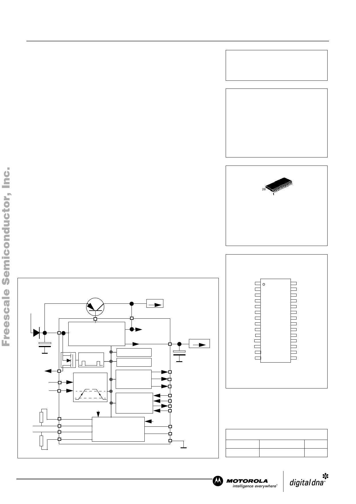
Simplified Block Diagram
Q1 5V
V2CTRL
V2
Vsup monitor
Dual Voltage Regulator
CAN
supply
Vdd1 Monitor
5V/200mA
HS1 control
Mode control
Oscillator
Programmable
wake-up input
Interrupt
Watchdog
Reset
Vsup
SPI Interface
Low Speed 125Kbit/s
Fault Tolerant CAN
Physical Interface
V2
Vdd1 5V/200mA
INTB
WDOGB
Reset
MOSI
SCLK
MISO
CSB
Txd
Rxd
Gnd
RX 1
TX 2
Vdd1 3
Reset 4
INTB 5
GND 6
GND 7
GND 8
GND 9
V2ctrl 10
Vsup 11
HS1 12
L0 13
L1 14
28 WDOGB
27 CSB
26 MOSI
25 MISO
24 SCLK
23 GND
22 GND
21 GND
20 GND
19 CANL
18 CANH
17 Rtl
16 Rth
15 V2
ORDERING INFORMATION
Device
Operating
Temperature Range
Package
PC33889DW TA = -40 to 125°C SO-28
Ttohcishdaongcuemoer ndtisccoonntatininuseinthfoisrmpraotidouncot nwiathporuotdnuoctticuen.deFr oderveMlopomreent. MInotfoororlamresaetrvieos ntheOrignht This Product,
Go to: www.freescale.com
© Motorola, Inc., 2002. All rights reserved.
1 page 
PC33889
Freescale Semiconductor, Inc.
(Vsup From 5.5V to 18V and Tj from -40°C to 125°C) unless otherwise noted. For all pins except can related pins
Description
Low Level Output Voltage (I0=1.5mA)
High Level Output Voltage (I0=-250uA)
INT Pin
Low Level Output Voltage (I0=1.5mA)
High Level Output Voltage (I0=-250uA)
HS1: 150mA High side output pin
Rdson at Tj=25°C, and Iout -150mA
Rdson at Tj=125°C, and Iout -150mA
Rdson at Tj=125°C, and Iout -120mA
Output current limitation
Over temperature Shutdown
Leakage current
Output Clamp Voltage at Iout= -1mA
Symbol
Vol
Voh
Characteristics
Min
0
Vdd1-0.9
Typ
Max
0.9
Vdd1
Unit
V
Vol 0
Voh Vdd1-0.9
0.9
Vdd1
V
Rdson25
2.5 Ohms
Rdson125
5 Ohms
Ron125-2
4 5.5 Ohms
Ilim 200
500 mA
Ovt 155
190 °C
Ileak
10 uA
Vcl -1.5
-0.3 V
Cyclic sense period (refer to SPI)
T1
ms
Cyclic sense On time (refer to SPI)
T2
100 us
Timing accuracy (cyclic sense period and
on time)
Tacc
-30
+30 %
L0 and L1 inputs
L0 Negative Switching Threshold
Vth0n
1.7
tbd
3V
23
2 tbd 3.1
L0 Positive Switching Threshold
Vth0p
2.2
tbd
4V
2.5 4
2.5 tbd 4.1
L1 Negative Switching Threshold
Vth1n
2
2.5
3V
2.5 3 3.6
2.7 3.2 3.7
L1 Positive Switching Threshold
Vth1p
2.7
3.3
3.8 V
3 4 4.6
3.5 4.2 4.7
Hysteresis
Vhyst
0.6
1.3 V
tbd
Input current
Iin -10
10 uA
Wake up Filter Time (enable/disable
option on L0 input)
8 20 38 us
DIGITAL INTERFACE TIMING
SPI operation frequency
Freq
4 MHz
SCLK Clock Period
SCLK Clock High Time
SCLK Clock Low Time
Falling Edge of CS to Rising
Edge of SCLK
tpCLK
twSCLKH
twSCLKL
tlead
250
125
125
100
50
ns
ns
ns
ns
Falling Edge of SCLK to Rising Edge of
CS
tlag
100
50
ns
MOSI to Falling Edge of SCLK
Falling Edge of SCLK to MOSI
MISO Rise Time (CL = 220pF)
MISO Fall Time (CL = 220pF)
tSISU
40
25
ns
tSIH 40 25
ns
trSO 25 50 ns
tfSO 25 50 ns
Conditions
5.5v<Vsup<27V
Vsup>9V
Vsup>9V
5.5V<Vsup<9V
no inductive load drive capa-
bility
in sleep and stop modes
in sleep and stop modes
in sleep and stop mode
5.5V<Vsup<6V
6V<Vsup<18V
18V<Vsup<27V
5.5V<Vsup<6V
6V<Vsup<18V
18V<Vsup<27V
5.5V<Vsup<6V
6V<Vsup<18V
18V<Vsup<27V
5.5V<Vsup<6V
6V<Vsup<18V
18V<Vsup<27V
5.5V<Vsup<18V
18V<Vsup<27V
-0.2V < Vin < 40V
(If filter enable)
PC33889
For More Information On This Product,
Go to: www.freescale.com
5
5 Page 
PC33889
FreescalDeEVSICEeDmESiCcRoIPnTIOdNuctor, Inc.
Figure 3. Device Signal Waveforms
Tx high: RECESSIVE Bit
VTX
CANL
Tx low: DOMINANT Bit
Tx high: RECESSIVE Bit
5V
3.6V
CANH
Vdiff
VRX
Vth(rd)
tonRX
RECESSIVE Bit
DOMINANT Bit
Vth(dr)
toffTX
1.4V
0V
2.2V
0.7V
-2.9V
-5V
toffRX
RECESSIVE Bit
0.7VCC
0.3VCC
t
Figure 4. Test Circuit for AC Characteristics
CANL
CANH
VDD
R
C
C
RC
R = 100ohms
C = 1nF
PC33889
For More Information On This Product,
Go to: www.freescale.com
11
11 Page | ||
| Páginas | Total 30 Páginas | |
| PDF Descargar | [ Datasheet PC33889.PDF ] | |
Hoja de datos destacado
| Número de pieza | Descripción | Fabricantes |
| PC3388 | IR ReceiverModules | PengCheng Elec-tech |
| PC33880 | Configurable Octal Serial Switch | Motorola Semiconductor |
| PC33887VW | 5.0 A H-Bridge with Load Current Feedback | Motorola Inc |
| PC33888APNB | Quad High-Side and Octal Low-Side Switch for Automotive | Motorola Inc |
| Número de pieza | Descripción | Fabricantes |
| SLA6805M | High Voltage 3 phase Motor Driver IC. |
Sanken |
| SDC1742 | 12- and 14-Bit Hybrid Synchro / Resolver-to-Digital Converters. |
Analog Devices |
|
DataSheet.es es una pagina web que funciona como un repositorio de manuales o hoja de datos de muchos de los productos más populares, |
| DataSheet.es | 2020 | Privacy Policy | Contacto | Buscar |