|
|
|
PDF QL4016-2CF100C Data sheet ( Hoja de datos )
| Número de pieza | QL4016-2CF100C | |
| Descripción | 16/000 Usable PLD Gate QuickRAM ESP Combining Performance/ Density and Embedded RAM | |
| Fabricantes | ETC | |
| Logotipo | ||
Hay una vista previa y un enlace de descarga de QL4016-2CF100C (archivo pdf) en la parte inferior de esta página. Total 18 Páginas | ||
|
No Preview Available !
QL4016 QuickRAM Data Sheet
• • • • • • 16,000 Usable PLD Gate QuickRAM ESP Combining Performance,
Density and Embedded RAM
Device Highlights
High Performance & High Density
• 16,000 Usable PLD Gates with 118 I/Os
• 300 MHz 16-bit Counters, 400 MHz
Datapaths, 160+ MHz FIFOs
• 0.35 µm four-layer metal non-volatile
CMOS process for smallest die sizes
High Speed Embedded SRAM
• 10 dual-port RAM modules, organized in
user-configurable 1,152 bit blocks
• 5 ns access times, each port independently
accessible
• Fast and efficient for FIFO, RAM, and ROM
functions
Easy to Use / Fast Development
Cycles
• 100% routable with 100% utilization and
complete pin-out stability
• Variable-grain logic cells provide high
performance and 100% utilization
• Comprehensive design tools include high
quality Verilog/VHDL synthesis
Advanced I/O Capabilities
• Interfaces with both 3.3 V and 5.0 V devices
• PCI compliant with 3.3 V and 5.0 V busses
for -1/-2/-3/-4 speed grades
• Full JTAG boundary scan
• I/O Cells with individually controlled
Registered Input Path and Output Enables
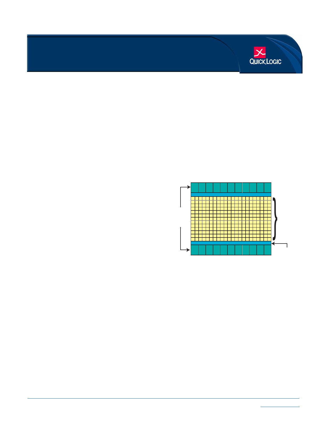
10
RAM
Blocks
320
High Speed
Logic Cells
Interface
Figure 1: QuickRAM Block Diagram
© 2002 QuickLogic Corporation
www.quicklogic.com
•
•
•
•
1
•
•
1 page 
QL4016 QuickRAM Data Sheet Rev I
[8:0]
[17:0]
[1:0]
WA RE
WD
WE
WCL K
MOD E
RCLK
[8:0]
RA
[17:0]
RD
ASYNCRD
Figure 4: QuickRAM Module
Symbol
tSWA
tHWA
tSWD
tHWD
tSWE
tHWE
tWCRD
Table 2: RAM Cell Synchronous Write Timing
Parameter
Propagation Delays (ns)
Fanout
12345
WA Setup Time to WCLK
1.0 1.0 1.0 1.0 1.0
WA Hold Time to WCLK
0.0 0.0 0.0 0.0 0.0
WD Setup Time to WCLK
1.0 1.0 1.0 1.0 1.0
WD Hold Time to WCLK
0.0 0.0 0.0 0.0 0.0
WE Setup Time to WCLK
1.0 1.0 1.0 1.0 1.0
WE Hold Time to WCLK
0.0 0.0 0.0 0.0 0.0
WCLK to RD (WA=RA)a
5.0 5.3 5.6 5.9 7.1
a. Stated timing for worst case Propagation Delay over process variation at VCC = 3.3 V and
TA = 25° C. Multiply by the appropriate Delay Factor, K, for speed grade, voltage and temperature
settings as specified in the Operating Range.
Symbol
Logic Cells
tSRA
tHRA
tSRE
tHRE
tRCRD
Table 3: RAM Cell Synchronous Read Timing
Parameter
Propagation Delays (ns)
Fanout
12345
RA Setup Time to RCLK
1.0 1.0 1.0 1.0 1.0
RA Hold Time to RCLK
0.0 0.0 0.0 0.0 0.0
RE Setup Time to RCLK
1.0 1.0 1.0 1.0 1.0
RE Hold Time to RCLK
RCLK to RDa
0.0 0.0 0.0 0.0 0.0
4.0 4.3 4.6 4.9 6.1
a. Stated timing for worst case Propagation Delay over process variation at VCC = 3.3 V and
TA = 25 × C. Multiply by the appropriate Delay Factor, K, for speed grade, voltage and temperature
settings as specified in the Operating Range.
© 2002 QuickLogic Corporation
•
www.quicklogic.com
••
•
•
•
5
5 Page 
Power-up Sequencing
QL4016 QuickRAM Data Sheet Rev I
VCCIO
VCC
(VCCIO -VCC)MAX
VCC
400 us
Time
Figure 8: Power-up Requirements
The following requirements must be met when powering up the device (refer to Figure 8):
• When ramping up the power supplies keep (VCCIO -VCC)MAX ≤ 500 mV. Deviation from
this recommendation can cause permanent damage to the device.
• VCCIO must lead VCC when ramping the device.
• The power supply must take greater than or equal to 400 µs to reach VCC. Ramping
to VCC/VCCIO earlier than 400 µs can cause the device to behave improperly.
An internal diode is present in-between VCC and VCCIO, as shown in Figure 9.
V CC
V CCIO
Internal Logic
Cells, RAM
blocks, etc
IO Cells
Figure 9: Internal Diode Between VCC and VCCIO
© 2002 QuickLogic Corporation
•
www.quicklogic.com
••
•
•
•
11
11 Page | ||
| Páginas | Total 18 Páginas | |
| PDF Descargar | [ Datasheet QL4016-2CF100C.PDF ] | |
Hoja de datos destacado
| Número de pieza | Descripción | Fabricantes |
| QL4016-2CF100C | 16/000 Usable PLD Gate QuickRAM ESP Combining Performance/ Density and Embedded RAM | ETC |
| QL4016-2CF100I | 16/000 Usable PLD Gate QuickRAM ESP Combining Performance/ Density and Embedded RAM | ETC |
| QL4016-2CF100M | 16/000 Usable PLD Gate QuickRAM ESP Combining Performance/ Density and Embedded RAM | ETC |
| Número de pieza | Descripción | Fabricantes |
| SLA6805M | High Voltage 3 phase Motor Driver IC. |
Sanken |
| SDC1742 | 12- and 14-Bit Hybrid Synchro / Resolver-to-Digital Converters. |
Analog Devices |
|
DataSheet.es es una pagina web que funciona como un repositorio de manuales o hoja de datos de muchos de los productos más populares, |
| DataSheet.es | 2020 | Privacy Policy | Contacto | Buscar |