|
|
|
PDF PBL385711NS Data sheet ( Hoja de datos )
| Número de pieza | PBL385711NS | |
| Descripción | High current Speech and Line interface Circuit | |
| Fabricantes | Ericsson | |
| Logotipo | ||
Hay una vista previa y un enlace de descarga de PBL385711NS (archivo pdf) en la parte inferior de esta página. Total 14 Páginas | ||
|
No Preview Available !
PBJLun3e81597991
PBL 385 71
High current Speech and
Line interface Circuit
Description.
Key features.
PBL 38571 is a monolithic integrated speech transmission circuit for use in
• Minimum number of external
electronic telephones and as DECT line interface with balanced in - and output. It is
components, 5 capacitors and 10
designed to accomodate either a low impedance dynamic microphone or an electret
resistors.
microphone that can be supplied from the circuits own DC - supply. A signal summing • Easy adaption to various market
point at the transmitter input is available. An internally preset line length
needs.
compensation can be adjusted with external resistors to fit into different current feed • Mute control input for operation with
systems as for ex. 48 V, 2 x 200 ohms, 48 V, 2 x 400 ohms and 48 V, 2 x 800
DTMF - generator.
ohms.The line regulation can be shut off in low mode. Application dependent para-
• Transmitter and receiver gain
meters such as line balance, side tone level, transmitter and receiver gains and
regulation for automatic loop loss
frequency responces are set independently by external components which means an
compensation. Disconnectable.
easy adaption to various market needs. The setting of the parameters, if carried out in • Extended current and voltage range
certain order will counteract the interaction between the settings. It features high line
5 - 130 mA, down to 2 V.
current capability on a small footprint. Function compatible with the PBL 3781 family • Differential microphone input for
of speech circuits.
good balance to ground.
• Balanced receiver output stage.
• In 16 - pin DIP and SO BW batwing
packages.
• Short start up time.
• Excellent RFI performance.
10
AM
11
1
PBL 385 71
AT AR
15
87 9 3
2
4,5, 16
12,13.
14 + 6
REC
Mute
(active low)
4
2
3
+
1
Telephone
line
16-pin plastic BW SO
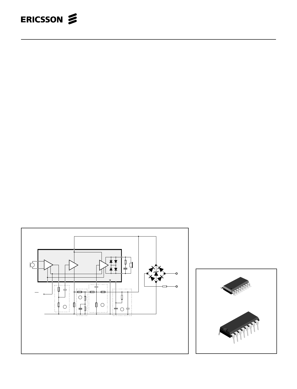
1. Impedance to the line and radio interference suppression
2. Transmitter gain and frequency responce network
3. Receiver gain and frequency responce network
4. Sidetone balance network
Figure 1. Functional diagram.
16-pin plastic BW DIP
1
1 page 
PBL 385 71
Functional description
Design procedure; ref. to fig.4.
+Line
The design is made easier through that all
settable parameters are returned to gro-
und (-line), this feature differs it from
bridge type solutions.To set the parameters
in the following order will result in that the
interaction between the same is minimized.
1. Set the circuit impedance to the line,
either resistive (600Ω) or complex. (R3
and C1). C1 should be big enough to give
low impedance compared with R3 in the
telephone speech frequency band.Too
large C1 will make the start-up slow. See
fig. 6.
2. Set the DC-characteristic that is
required in the PTT specification or in
case of a system telephone,in the PBX
specification (R6).There are also internal
circuit dependent requirements like supply
voltages etc.
3. Set the attac point where the line
length regulation is supposed to cut in
(R1 and R2 in fig. 18). Note that in some
countries the line length regulation is not
allowed. In most cases the end result is
better and more readily achieved by using
the line length regulation (line loss
compensation) than without. See fig. 13.
4.Set the transmitter gain and
frequency response.
5. Set the receiver gain and frequency
response. See text how to limit the max.
swing to the earphone.
6. Adjust the side tone balancing
network.
7. Set the RFI suppression
components in case necessary. In two
piece telephones the often ”helically”
wound cord acts as an aerial. The
microphone input with its high gain is
especially sensitive.
8. Circuit protection. Apart from any
other protection devices used in the de-
sign, a good practice is to connect a 15V
1W zener diode across the circuit , from
pin 1 to -Line.
1
+
AM 2
Transmitter summing
input
Mute
Figure 7. Block connections.
PBL 38 571
1
6
3
C2
2
R6
Figure 6. AC-impedance.
Impedance to the line
The AC- impedance to the line is
set by R3, C1 and C2. Fig.4. The circuits
relatively high parallel impedance will not
influence it to any noticeable extent. At low
frequencies the influence of C1 can not be
neglected. Series resistance of C1 that is
dependent on the temperature and the
quality of the component will cause some
of the line signal to enter pin 6. This
generates a closed loop in the transmitter
amplifier that in it´s turn will create an
active impedance thus lowering the
impedance to the line. The impedance at
high frequencies is set by C2 that also
acts as a RFI suppressor.
In many specifications the
impedance towards the line is specified as
a complex network. See fig. 6. In case a).
the error signal entering pin 6 is set by the
ratio ≈Rs/R19 (910Ω), where in case b).
the ratio at high frequencies will be Rs/
220Ω because the 820Ω resistor is
AT
4
3
+ Line
AR
- Line
a) b)
R3
c)
220Ω
820Ω
Cx
Rs
≈1Ω
+
C1
Example:
How to connect a
complex network.
220Ω+820Ω//Cx
-Line
bypassed by a capacitor. To help up this
situation the complex network capacitor is
connected directly to ground, case c).
making the ratio Rs/220Ω+820Ω and thus
lessening the error signal. Conclusion:
Connect like in case c) when complex
impedance is specified.
DC - characteristic
The DC - characteristic that a
telephone set has to fulfill is mainly given
by the network administrator. Following
parameters are useful to know when the
DC behaviour of the telephone is to be set:
• The voltage of the feeding system
• The line feeding resistance 2 x.......
ohms.
• The maximum current from the line at
zero line length.
• The min. current at which the telephone
has to work (basic function).
• The lowest and highest voltage
permissible across the telephone set.
• The highest voltage that the
telephone may have at different line
currents. Normally set by the
network owners specification.The
lowest voltage for the telephone is
normally set by the voltages that are
needed for the different parts of the
telephone to function. For ex. for
transmitter output amplifier, recei-
ver output amplifier, dialler, speech
switching.
5
5 Page 
PBL 385 71
Power supply V+C. (See fig.18)
PBL 385 71 generates its own DC
supply V+C dependent of line current with
an internal shunt regulator. This regulator
senses the line voltage VL via R3 and line
current via R6 in order to set the correct
V+C so the circuit can generate the required
DC characteristic for a given line resistance
RLine and the line feeding data of the
exchange. A decoupling capacitor is
needed between pins +C and -L. The V+C
supply changes its voltage linearly with the
line current. It can be used to feed an
electret microphone. Caution must be ta-
ken though not to drain too much current
out of this output because it will affect the
internal quick start circuit by locking itself
into active state. (max. permissible current
drain 700µA)
Care has to be taken when deci-
ding the resistance value of R3. See fig.6.
All resistances that are applied from +Line
to ground (-Line) will be in parallel, forming
the real impedance towards the line. This
will sometimes result in, that the ohmic
value of R3 is increased in order to comply
to the impedance specification towards
the line. The speech circuit sinks ≈ 1mA
into pin 6, which means that the working
voltage for the speech function V+ will
decrease with increasing R3, thus starving
in the end the circuit of its working voltage
. This dependency is often falsely taken as
a sign of that the circuit does not work
down to the low line current specified, but
in fact it is the working voltage at pin 6 that
has become too low. It is obvious that this
problem is also connected into what kind
of DC-characteristic is set. See fig. 8.
1-5M
VDD
CMOS
DIALLER
+
47µF
MUTE
DTMF
GND
12 3
456
789
*0 #
15k
5.1V
200Ω
MIC.
200 Ω
1
1µF
10
AM
11 +
1µF
87
9
PBL 385 71
AT AR
32
4,5,
12,13
14
R2
+
100 µF
1k
910Ω
18k
100nF
22k
R1
75 Ω
100nF
6.2k
560Ω
11k
47nF
62k
11k
15
16
+6
100 Ω
1nF
R3
910 Ω
+ C1
47µ F
C2
15nF
15V
1W
Hook
switch
1N4007
1N4007
1N4007
1N4007
Teleph
line
10Ω
Figure 18. Typical standard DTMF dialling telephone application.
11
11 Page | ||
| Páginas | Total 14 Páginas | |
| PDF Descargar | [ Datasheet PBL385711NS.PDF ] | |
Hoja de datos destacado
| Número de pieza | Descripción | Fabricantes |
| PBL385711NS | High current Speech and Line interface Circuit | Ericsson |
| Número de pieza | Descripción | Fabricantes |
| SLA6805M | High Voltage 3 phase Motor Driver IC. |
Sanken |
| SDC1742 | 12- and 14-Bit Hybrid Synchro / Resolver-to-Digital Converters. |
Analog Devices |
|
DataSheet.es es una pagina web que funciona como un repositorio de manuales o hoja de datos de muchos de los productos más populares, |
| DataSheet.es | 2020 | Privacy Policy | Contacto | Buscar |