|
|
|
PDF RF2488 Data sheet ( Hoja de datos )
| Número de pieza | RF2488 | |
| Descripción | MULTI-MODE DUAL-BAND LNA MIXER | |
| Fabricantes | RF Micro Devices | |
| Logotipo | ||
Hay una vista previa y un enlace de descarga de RF2488 (archivo pdf) en la parte inferior de esta página. Total 22 Páginas | ||
|
No Preview Available !
Preliminary
8
RF2488
MULTI-MODE DUAL-BAND LNA MIXER
Typical Applications
• TDMA/EDGE Handsets
• TDMA IS-136 Handsets
• GAIT Handsets
• TDMA/GSM Dual-Band Handsets
• GSM/DCS/EDGE Handsets
Product Description
The RF2488 is a dual-band LNA/Mixer designed to sup-
port dual-band, multi-mode handset applications. The
unique dual IF outputs provide interface to two indepen-
dent IF SAW filters supporting applications that combine
IS136 with GSM, DCS or EDGE air interfaces. The device
includes four mixers, providing the ability to use two inde-
pendent IF bandwidths accessible from either the low or
high band LNAs. Each LNA has a gain bypass mode con-
trolled by the GAIN SEL pin. An image reject filter is
required between each LNA and its mixer. Power man-
agement is implemented based on a three-pin logic level
interface. Power consumption is minimized by shutting
down all but the active sections of the device.
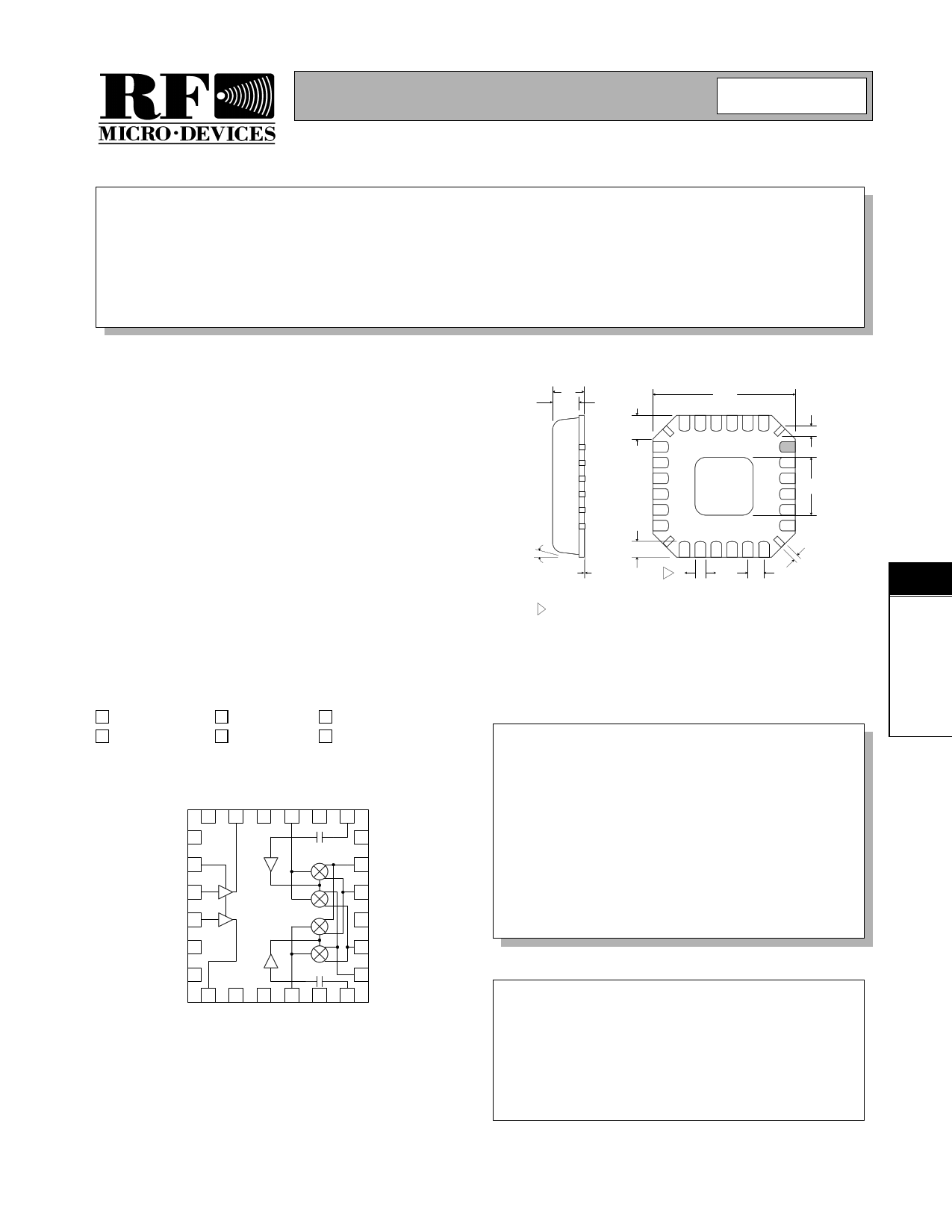
1.00
.80 0.85
.65
.60
.24
typ
4.00
sq.
.45
.20
4 PLCS
2.25
1.95
sq.
12° .55
max .30
.05
.01
.40
2 .28
.50
NOTES:
1 Shaded Pin is Lead 1.
2 Dimension applies to plated terminal: to be measured between 0.02 mm
and 0.25 mm from terminal end.
3 Pin 1 identifier must exist on top surface of package by identification
mark or feature on the package body. Exact shape and size is optional.
4 Package Warpage: 0.05 mm max.
5 Die Thickness Allowable: 0.305 mm max.
.23
.13
4 PLCS
Optimum Technology Matching® Applied
Si BJT
Si Bi-CMOS
GaAs HBT
üSiGe HBT
GaAs MESFET
Si CMOS
24 23 22 21 20 19
Low
LNA GND
1
18 BAND SEL
GAIN SEL 2
17 IF1+
Low
LNA IN
3
16 IF1-
High
LNA IN
4
15 MXR VCC
High
LNA GND
5
14 IF2+
High
LNA VCC
6
13 IF2-
7 8 9 10 11 12
Package Style: LCC, 24-Pin, 4x4
Features
• Complete Dual-Band Front-End
• Switchable LNA Gain
• Low Noise and High Intercept Point
• Low Current Consumption
• Single 2.7V to 3.3V Power Supply
• Supports Dual IF Bandwidths
Ordering Information
RF2488
Multi-Mode Dual-Band LNA Mixer
RF2488 PCBA Fully Assembled Evaluation Board
Functional Block Diagram
RF Micro Devices, Inc.
7625 Thorndike Road
Greensboro, NC 27409, USA
Tel (336) 664 1233
Fax (336) 664 0454
http://www.rfmd.com
8
Rev A0 010905
8-123
1 page 
Preliminary
RF2488
Pin Function Description
Interface Schematic
1 Low LNA Low band LNA ground connection. As an option, an external inductor to See pin 3.
GND
ground may be used to reduce LNA gain.
2 GAIN SEL CMOS compatible signal controlling both the low band and high band
LNA gain. Logic (0)=Low Gain, Logic (1)=High Gain.
3 Low LNA IN Low band LNA input. The maximum VSWR is 2:1 (Cell/GSM RX band)
for both the gain and bypass mode. This pin is internally DC-biased
and should be DC blocked with a capacitor suitable for the frequency of
operation.
Low LNA IN
Low LNA OUT
4 High LNA IN High band LNA input. The maximum VSWR is 2:1 (DCS/PCS RX band)
for both the gain and bypass mode. This pin is internally DC-biased
and should be DC blocked with a capacitor suitable for the frequency of
operation.
High LNA IN
Low LNA GND
High LNA OUT
5 High LNA High band LNA ground connection. Immediate grounding required See pin 4.
GND
adjacent to pin.
6 High LNA High band LNA supply voltage. Local bypass capacitor required.
VCC
7 High LNA High band LNA Output. Bias for the LNA is provided through this pin, See pin 4.
OUT
hence it should be connected to VCC through an inductor.
8
GND
Direct connection to ground.
9 IF OUT SEL IF output select state control pin. This CMOS compatible signal con-
trols the selection of the IF mixer output path (see the State Control
Truth Table). Local bypass capacitor required.
10 High MIX IN High band RF mixer input. Although the base of the mixer input transis-
tor is AC coupled, this pin serves a dual purpose of providing a DC-bias
path via external inductor to GND. The typical input impedance is 8Ω
High MIX IN
real and requires external matching to 50Ω.
High LNA GND
11 NC
12 High LO IN High band local oscillator input. This pin is internally AC-coupled and See pin 19.
matched to 50Ω.
13
IF2-
IF output. Open collector output, requires external matching compo-
nents and DC connection to VCC.
IF2+
IF2-
1 pF
1 pF 1 pF
8
14
IF2+
IF output. Open collector output, requires external matching compo- See pin 13.
nents and DC connection to VCC.
15 MXR VCC Mixer supply voltage. Local bypass capacitor required.
Rev A0 010905
8-127
5 Page 
Preliminary
RF2488
Evaluation Board Schematic
IF @ 135 MHz
(Download Bill of Materials from www.rfmd.com.)
FL1*
Saw Filter
I/O I/O
R2* R3*
0Ω 0Ω
L2
4.7 nH
R4
0Ω
J1
LNA1 OUT
LNA1 VCC
GAIN SEL
J4
LNA1 IN
J5
LNA2 IN
J8
LNA2 OUT
50 Ω µstrip
R1
0Ω
C1 L1
1.2 pF 15 nH
Bias VCC C10
5 pF
C2
100 pF
L6
4.7 nH
C4
100 pF
C5
100 pF
L8 C13
56 nH 33 nF
TRL
50 Ω µstrip
50 Ω µstrip
L10
2.2 nH
C12
33 nF
C11*
DNI
L9*
DNI
TRL
LNA2 VCC
24 23 22 21 20 19
1 18
2 17
3 16
4 15
5 14
6 13
7 8 9 10 11 12
50 Ω µstrip
C8
10 pF
L17
10 nH
L4
12 nH
R5
0Ω
C24
100 pF
2488400-
C9
100 pF
L7
8.2 nH
C25
3 pF (HQ)
R6*
0Ω
R7*
0Ω
I/O I/O
IF OUT
SELECT
C3
100 pF
L3
2.2 nH
C6
100 pF
L11
180 nH
C14
10 pF
L15
560 nH
R9
820 Ω
C20
1 nF
C15
10 pF
C19
1 nF
MX VCC
C16
10 pF
L12
180 nH
L5
2.2 nH
R8
0Ω
C17
10 pF
C7
100 pF
C18
1 nF
L16
560 nH
R10
820 Ω
C21
1 nF
VCC
P1
1
FL2*
Saw Filter
JP1
NOTE: Parts with * after reference designator should not be populated on evaluation board.
12
2
CON2
GND
3
5
4
6
78
9 10
11 12
13 14
C26 + C27
1 µF
1 nF
15
HEADER 8X2
16
C28
1 nF
R11
10 kΩ
C29
1 nF
R12
10 kΩ
C30
1 nF
C31
1 nF
R13
10 kΩ
C32
1 nF
R14
10 kΩ
50 Ω µstrip
J2
MX1 IN
50 Ω µstrip
L13
180 nH
C22
8 pF
50 Ω µstrip
TX/RX
J3
LO1 IN
Band Select
J7
IF1 OUT
C23
8 pF
L14
180 nH
50 Ω µstrip
50 Ω µstrip
50 Ω µstrip
J6
IF2 OUT
J9
LO2 IN
J10
MX2 IN
LNA1 VCC
LNA2 VCC
MX VCC
IF Out Select
Gain Select
Bias VCC
Band Select
C33
1 nF
C34
1 nF
TX/RX
C35
1 nF
8
Rev A0 010905
8-133
11 Page | ||
| Páginas | Total 22 Páginas | |
| PDF Descargar | [ Datasheet RF2488.PDF ] | |
Hoja de datos destacado
| Número de pieza | Descripción | Fabricantes |
| RF2480 | DIRECT QUADRATURE MODULATOR | RF Micro Devices |
| RF2483 | LOW NOISE DUAL-BAND QUADRATURE MODULATOR WITH AGC | RF Micro Devices |
| RF2484 | DIRECT QUADRATURE MODULATOR | RF Micro Devices |
| RF2485 | VHF QUADRATURE MODULATOR | RF Micro Devices |
| Número de pieza | Descripción | Fabricantes |
| SLA6805M | High Voltage 3 phase Motor Driver IC. |
Sanken |
| SDC1742 | 12- and 14-Bit Hybrid Synchro / Resolver-to-Digital Converters. |
Analog Devices |
|
DataSheet.es es una pagina web que funciona como un repositorio de manuales o hoja de datos de muchos de los productos más populares, |
| DataSheet.es | 2020 | Privacy Policy | Contacto | Buscar |