|
|
|
PDF PALC22V10D Data sheet ( Hoja de datos )
| Número de pieza | PALC22V10D | |
| Descripción | FLASG ERASABLE REPROGRAMMABLE CMOS PAL DEVICE | |
| Fabricantes | Cypress Semiconductor | |
| Logotipo | ||
Hay una vista previa y un enlace de descarga de PALC22V10D (archivo pdf) en la parte inferior de esta página. Total 11 Páginas | ||
|
No Preview Available !
For new designs, please refer to the PALCE22V10.
PALC22V10D
Features
D Advanced secondĆgeneration PAL arĆ
chitecture
D Low power
Ċ 90 mA max. commercial (10 ns)
Ċ 130 mA max. commercial (7.5 ns)
D CMOS Flash EPROM technology for
electrical erasability and reprogramĆ
mability
D Variable product terms
Ċ 2 xĂ(8 through ā16) product terms
D UserĆprogrammable macrocell
Ċ Output polarity control
Ċ Individually selectable for regisĆ
tered or combinatorial operation
D Up to 22 input terms and 10 outputs
Flash Erasable,
Reprogrammable CMOS PALR Device
D DIP, LCC, and PLCC available
Ċ 7.5 ns commercial version
5 ns tCO
5 ns tS
7.5 ns tPD
133ĆMHz state machine
Ċ 10 ns military and industrial verĆ
sions
6 ns tCO
6 ns tS
10 ns tPD
110ĆMHz state machine
Ċ 15Ćns commercial and military
versions
Ċ 25Ćns commercial and military
versions
D High reliability
Ċ Proven Flash EPROM technology
Ċ 100% programming and functional
testing
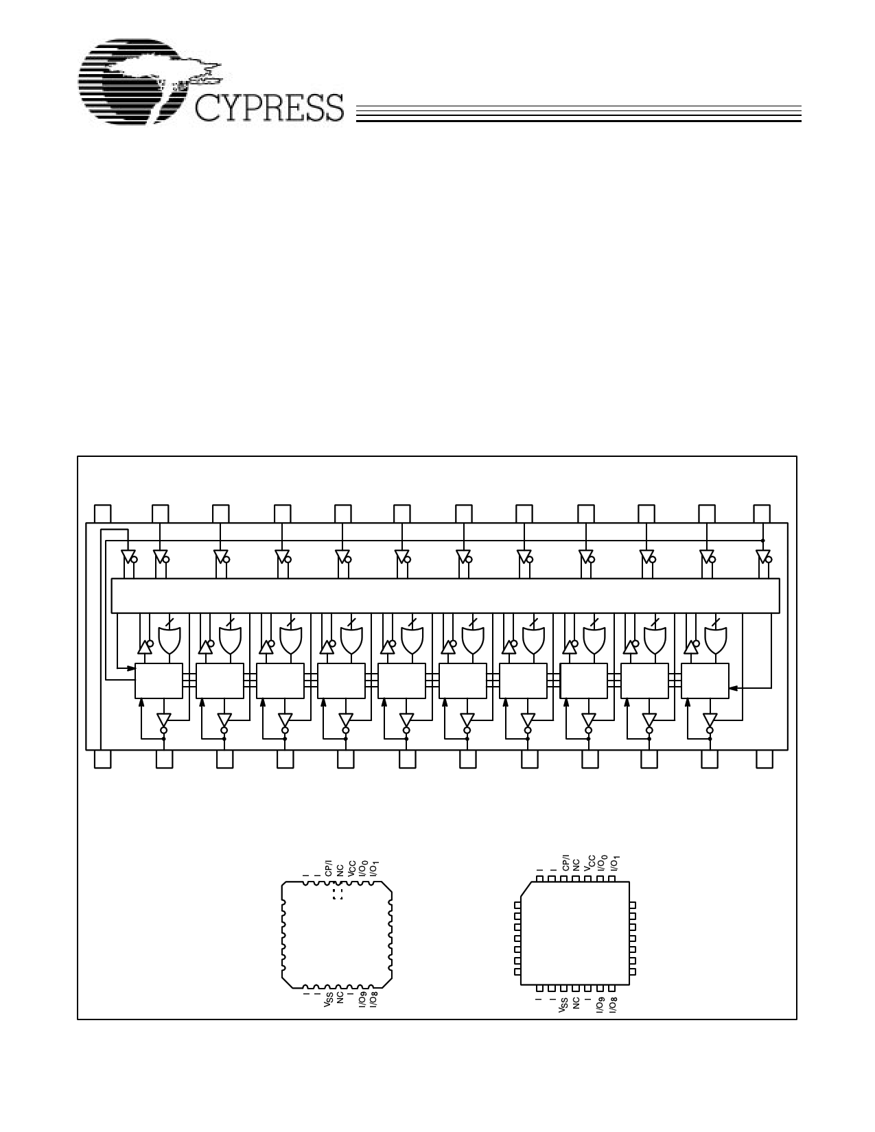
Functional Description
The Cypress PALC22V10D is a CMOS
Flash Erasable secondĆgeneration proĆ
grammable array logic device. It is imĆ
plemented with the familiar sumĆofĆproĆ
ducts (ANDĆOR) logic structure and the
programmable macrocell.
The PALC22V10D is executed in a 24Ćpin
300Ćmil molded DIP, a 300Ćmil cerDIP, a
28Ćlead square ceramic leadless chip carriĆ
er, a 28Ćlead square plastic leaded chip carĆ
rier, and provides up to 22 inputs and 10
outputs. The 22V10D can be electrically
Logic Block Diagram (PDIP/CDIP)
VSS
I
II
I
12 11
10
98
I
7
II
65
II
43
I CP/I
21
8 10
12 14
PROGRAMMABLE
AND ARRAY
(132 X 44)
16 16
14
12 10
8
Reset
Macrocell
Macrocell
Macrocell
Macrocell
Macrocell
Macrocell
Macrocell
Macrocell
Macrocell
Macrocell
Preset
13 14 15
I
I/O9
I/O8
Pin Configuration
16
I/O 7
17
I/O6
LCC
Top View
18
I/O5
19
I/O4
20
I/O3
21
I/O2
22
I/O1
PLCC
Top View
23
I/O0
24
VCC
V10DĆ1
I
I
I
NC
I
I
I
4 3 2 1 28 27 26
5 25
6 24
7 23
8 22
9 21
10 20
11 19
12 13 14 15 16 17 18
I/O 2
I/O 3
I/O 4
N/C
I/O 5
I/O 6
I/O 7
V10DĆ2
PAL is a registered trademark of Advanced Micro Devices.
I
I
I
NC
I
I
I
4 3 2 1 28 27 26
5 25
6 24
7 23
8 22
9 21
10 20
11 19
12 13 14 15 16 17 18
I/O 2
I/O 3
I/O 4
N/C
I/O 5
I/O 6
I/O 7
V10DĆ3
DCypress Semiconductor Corporation
3901 North First Street
1
D DSan Jose
DCA 95134
408-943-2600
July 1991 - Revised October 1995
1 page 
PALC22V10D
Commercial Switching Characteristics PALC22V10D[2, 7]
22V10D-7 22V10D-10 22V10D-15 22V10D-25
Parameter
Description
Min. Max. Min. Max. Min. Max. Min. Max. Unit
tPD
tEA
tER
tCO
tS1
tS2
tH
tP
tWH
tWL
fMAX1
fMAX2
fMAX3
tCF
Input to Output
Propagation Delay[8, 9]
3 7.5 3 10 3 15 3 25 ns
Input to Output Enable Delay[10]
8
10 15 25 ns
Input to Output Disable Delay[11]
8
10 15 25 ns
Clock to Output Delay[8, 9]
2 5 2 7 2 8 2 15 ns
Input or Feedback SetĆUp Time
5
6 10 15 ns
Synchronous Preset SetĆUp Time
6
7 10 15 ns
Input Hold Time
0 0 0 0 ns
External Clock Period (tCO + tS)
10
12
20
30
Clock Width HIGH[6]
3 3 6 13
Clock Width LOW[6]
3 3 6 13
ns
ns
ns
External Maximum Frequency
(1/(tCO + tS))[12]
100
76.9
55.5
33.3
MHz
Data Path Maximum Frequency
(1/(tWH + tWL))[6, 13]
166
142
83.3
35.7
MHz
Internal Feedback Maximum
Frequency (1/(tCF + tS))[6,Ă14]
133
111
68.9
38.5
MHz
Register Clock to
Feedback Input[6, 15]
2.5 3 4.5 13 ns
tAW
tAR
tAP
Asynchronous Reset Width
AsynchronousResetRecoveryTime
Asynchronous Reset to
Registered Output Delay
8
5
10 15 25
6 10 25
12 13 20 25
ns
ns
ns
tSPR
Synchronous Preset Recovery Time
6
tPR
Notes:
PowerĆUp Reset Time[6,Ă16]
1
7. Part (a) of AC Test Loads and Waveforms is used for all parameters exĆ
cept tER and tEA(+). Part (b) of AC Test Loads and Waveforms is used
for tER. Part (c) of AC Test Loads and Waveforms is used for tEA(+).
8. Min. times are tested initially and after any design or process changes
that may affect these parameters.
9. This specification is guaranteed for all device outputs changing state in
a given access cycle.
10. The test load of part (a) of AC Test Loads and Waveforms is used for
measuring tEA(-). The test load of part (c) of AC Test Loads and
Waveforms is used for measuring tEA(+) only. Please see part (e) of AC
Test Loads and Waveforms for enable and disable test waveforms and
measurement reference levels.
11. This parameter is measured as the time after output disable input that
the previous output data state remains stable on the output. This delay
is measured to the point at which a previous HIGH level has fallen to
0.5 volts below VOH min. or a previous LOW level has risen to 0.5 volts
above VOL max. Please see part (e) of AC Test Loads and Waveforms
for enable and disable test waveforms and measurement reference
levels.
8 10 15 ns
1 1 1 ms
12. This specification indicates the guaranteed maximum frequency at
which a state machine configuration with external feedback can
operate.
13. This specification indicates the guaranteed maximum frequency at
which the device can operate in data path mode.
14. This specification indicates the guaranteed maximum frequency at
which a state machine configuration with internal only feedback can
operate.
15. This parameter is calculated from the clock period at fMAX internal
(1/fMAX3) as measured (see Note 11 above) minus tS.
16. The registers in the PALC22V10D have been designed with the capaĆ
bility to reset during system powerĆup. Following powerĆup, all regisĆ
ters will be reset to a logic LOW state. The output state will depend on
the polarity of the output buffer. This feature is useful in establishing
state machine initialization. To insure proper operation, the rise in VCC
must be monotonic and the timing constraints depicted in PowerĆUp
Reset Waveform must be satisfied.
5
5 Page 
Package Diagrams (continued)
24ĆLead (300ĆMil) Molded DIP P13/P13A
PALC22V10D
E Cypress Semiconductor Corporation, 1995. The information contained herein is subject to change without notice.
Cypress Semiconductor Corporation assumes no responsibility for
the use of any circuitry other than circuitry embodied in a Cypress Semiconductor Corporation product. Nor does it convey or imply any license under patent or other rights. Cypress SemiconĆ
ductor does not authorize its products for use as critical components in lifeĆsupport systems where a malfunction or failure of the product may reasonably be expected to result in significant
11injury to the user. The inclusion of Cypress Semiconductor products in lifeĆsupport systems applications implies that the manufacturer assumes all risk of such use and in so doing indemnifies
Cypress Semiconductor against all damages.
11 Page | ||
| Páginas | Total 11 Páginas | |
| PDF Descargar | [ Datasheet PALC22V10D.PDF ] | |
Hoja de datos destacado
| Número de pieza | Descripción | Fabricantes |
| PALC22V10 | Reprogrammable CMOS PAL Device | Cypress Semiconductor |
| PALC22V10D | FLASG ERASABLE REPROGRAMMABLE CMOS PAL DEVICE | Cypress Semiconductor |
| Número de pieza | Descripción | Fabricantes |
| SLA6805M | High Voltage 3 phase Motor Driver IC. |
Sanken |
| SDC1742 | 12- and 14-Bit Hybrid Synchro / Resolver-to-Digital Converters. |
Analog Devices |
|
DataSheet.es es una pagina web que funciona como un repositorio de manuales o hoja de datos de muchos de los productos más populares, |
| DataSheet.es | 2020 | Privacy Policy | Contacto | Buscar |