|
|
|
PDF DS3893AV Data sheet ( Hoja de datos )
| NÚmero de pieza | DS3893AV | |
| DescripciÃģn | BTL TURBOTRANSCEIVERïŋ―ïŋ― | |
| Fabricantes | National Semiconductorã | |
| Logotipo | ||
Hay una vista previa y un enlace de descarga de DS3893AV (archivo pdf) en la parte inferior de esta pÃĄgina. Total 7 PÃĄginas | ||
|
No Preview Available !
March 1997
DS3893A
BTL TURBOTRANSCEIVERâĒ
General Description
The TURBOTRANSCEIVER is designed for use in very high
speed bus systems. The bus terminal characteristics of the
TURBOTRANSCEIVER are referred to as âBackplane
Transceiver Logicâ (BTL). BTL is a new logic signaling stan-
dard that has been developed to enhance the performance
of backplane buses. BTL compatible transceivers feature
low output capacitance drivers to minimize bus loading, a 1V
nominal signal swing for reduced power consumption and
receivers with precision thresholds for maximum noise im-
munity. This new standard eliminates the settling time de-
lays, that severely limit the TTL bus performance, to provide
significantly higher bus transfer rates.
The TURBOTRANSCEIVER is compatible with the require-
ments of the proposed IEEE 896 Futurebus draft standard. It
is similar to the DS3896/97 BTL TRAPEZOIDALâĒ Trans-
ceivers but the trapezoidal feature has been removed to
improve the propagation delay. A stripline backplane is there-
fore required to reduce the crosstalk induced by the faster
rise and fall times. This device can drive a 10âĶ load with a
typical propagation delay of 3.5 ns for the driver and 5 ns for
the receiver.
When multiple devices are used to drive a parallel bus, the
driver enables can be tied together and used as a common
control line to get on and off the bus. The driver enable delay
is designed to be the same as the driver propagation delay in
order to provide maximum speed in this configuration. The
low input current on the enable pin eases the drive required
for the common control line.
The bus driver is an open collector NPN with a Schottky
diode in series to isolate the transistor output capacitance
from the bus when the driver is in the inactive state. The
active output low voltage is typically 1V. The bus is intended
to be operated with termination resistors (selected to match
the bus impedance) to 2.1V at both ends. Each of the
resistors can be as low as 20âĶ.
Features
n Fast single ended transceiver (typical driver enable and
receiver propagation delays are 3.5 ns and 5 ns)
n Backplane Transceiver Logic (BTL) levels (1V logic
swing)
n Less than 5 pF bus-port capacitance
n Drives densely loaded backplanes with equivalent load
impedances down to 10âĶ
n 4 transceivers in 20 pin PCC package
n Specially designed for stripline backplanes
n Separate bus ground returns for each driver to minimize
ground noise
n High impedance, MOS and TTL compatible inputs
n TRI-STATEâĒ control for receiver outputs
n Built-in bandgap reference provides accurate receiver
threshold
n Glitch free power up/down protection on all outputs
n Oxide isolated bipolar technology
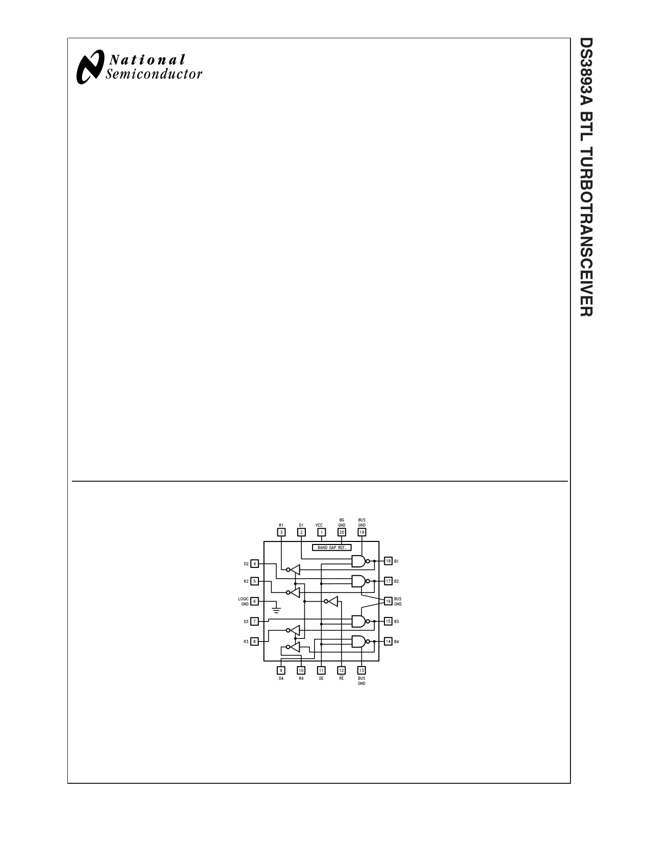
Connection and Logic Diagram
00869801
Order Number DS3893AV
See NS Package Number V20A
TRI-STATEÂŪ is a registered trademark of National Semiconductor Corporation.
TRAPEZOIDALâĒ and TURBOTRANSCEIVERâĒ are trademarks of National Semiconductor Corp.
ÂĐ 2004 National Semiconductor Corporation DS008698
www.national.com
1 page 
Switching Time Waveforms (Continued)
FIGURE 7. Receiver Propagation Delay
00869807
Note: tR = tF âĪ 4 ns From 10% to 90%
Note: n = 1, 2, 3, 4
FIGURE 8. Receiver Enable and Disable Times
Typical Application
00869808
Application Information
Due to the high current and very high speed capability of the
TURBOTRANSCEIVERâs driver output stage, circuit board
layout and bus grounding are critical factors that affect the
system performance.
Each of the TURBOTRANSCEIVERâs bus ground pins
should be connected to the nearest backplane ground pin
with the shortest possible path. The ground pins on the
connector should be distributed evenly through its length.
Although the bandgap reference receiver threshold provides
sufficient DC noise margin (Figure 9), ground noise and
ringing on the data paths could easily exceed this margin if
the series inductance of the traces and connectors are not
kept to a minimum. The bandgap ground pin should be
returned to the connector through a separate trace that does
00869809
not carry transient switching currents. The transceivers
should be mounted as close as possible to the connector. It
should be noted that even one inch of trace can add a
significant amount of ringing to the bus signal.
00869810
FIGURE 9. Noise Margin
5 www.national.com
5 Page | ||
| PÃĄginas | Total 7 PÃĄginas | |
| PDF Descargar | [ Datasheet DS3893AV.PDF ] | |
Hoja de datos destacado
| NÚmero de pieza | DescripciÃģn | Fabricantes |
| DS3893A | BTL TURBOTRANSCEIVER | National Semiconductor |
| DS3893A | DS3893A BTL TURBOTRANSCEIVER (Rev. D) | Texas Instruments |
| DS3893AV | BTL TURBOTRANSCEIVER | National Semiconductor |
| DS3893AV | BTL TURBOTRANSCEIVERïŋ―ïŋ― | National Semiconductor |
| NÚmero de pieza | DescripciÃģn | Fabricantes |
| SLA6805M | High Voltage 3 phase Motor Driver IC. |
Sanken |
| SDC1742 | 12- and 14-Bit Hybrid Synchro / Resolver-to-Digital Converters. |
Analog Devices |
|
DataSheet.es es una pagina web que funciona como un repositorio de manuales o hoja de datos de muchos de los productos mÃĄs populares, |
| DataSheet.es | 2020 | Privacy Policy | Contacto | Buscar |