|
|
|
PDF J108 Data sheet ( Hoja de datos )
| Número de pieza | J108 | |
| Descripción | N-Channel JFET Switch | |
| Fabricantes | Calogic LLC | |
| Logotipo | ||
Hay una vista previa y un enlace de descarga de J108 (archivo pdf) en la parte inferior de esta página. Total 1 Páginas | ||
|
No Preview Available !
CORPORATION
N-Channel JFET Switch
J108 – J110 / SST108 – SST110
FEATURES
Low Cost
• Automated Insertion Package
• Low Insertion Loss
•• No Offset or Error Voltages Generated by Closed Switch
Purely Resistive
High Isolation Resistance from Driver
Fast Switching
•• Low Noise
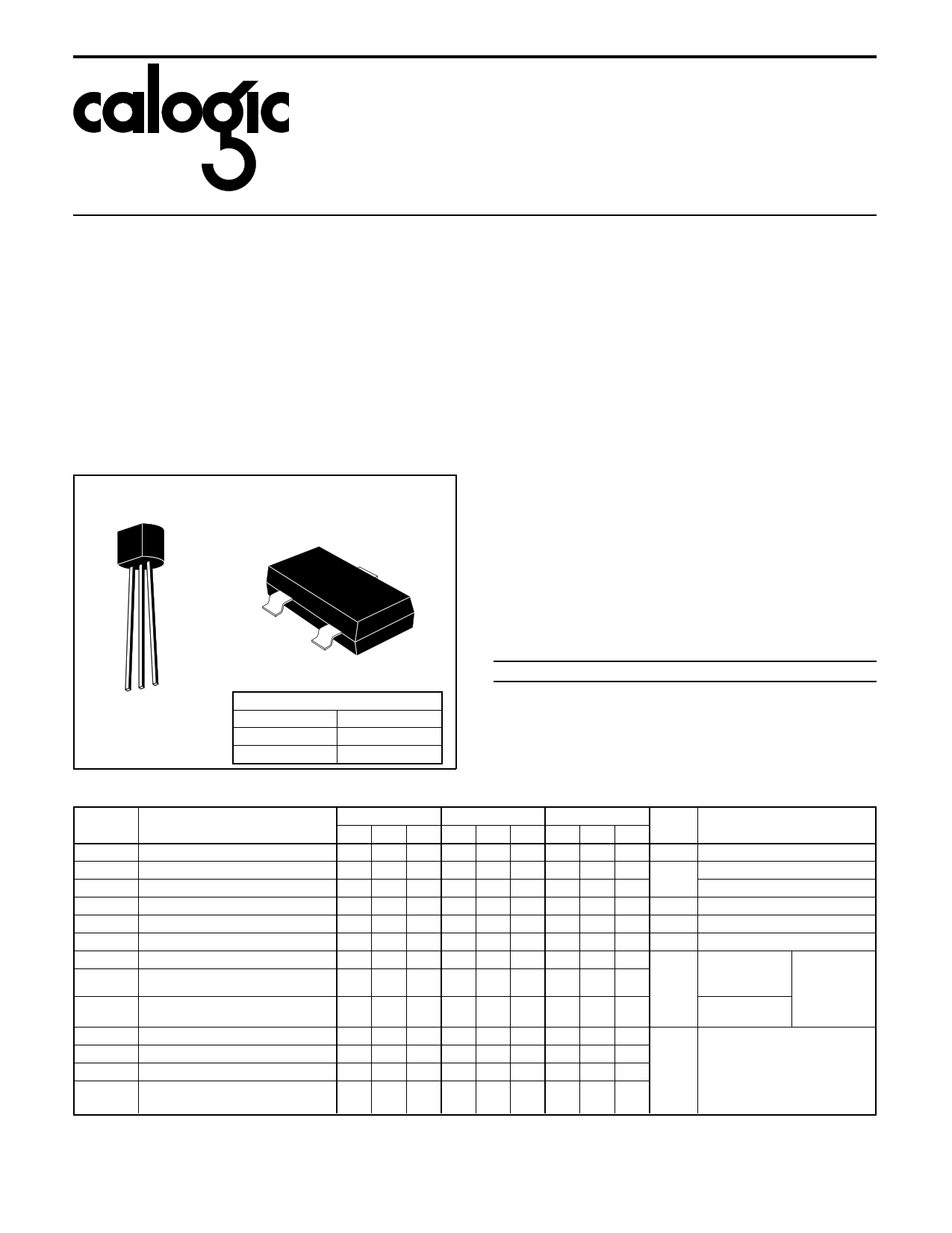
PIN CONFIGURATION
TO-92
D SG
5018
SOT-23
G
D
S
PRODUCT MARKING (SOT-23)
SST108
I08
SST109
I09
SST110
I10
APPLICATIONS
Analog Switches
• Choppers
• Commutators
•• Low-Noise Audio Amplifiers
A(TBAS=O2L5UoCTEunMleAsXsIMotUheMrwRisAeTsINpeGcSified)
Gate-Drain or Gate-Source Voltage . . . . . . . . . . . . . . . . -25V
Gate Current . . . . . . . . . . . . . . . . . . . . . . . . . . . . . . . . . 50mA
Storage Temperature Range . . . . . . . . . . . . . -55oC to +150oC
Operating Temperature Range . . . . . . . . . . . -55oC to +135oC
Lead Temperature (Soldering, 10sec) . . . . . . . . . . . . . +300oC
Power Dissipation . . . . . . . . . . . . . . . . . . . . . . . . . . . . 360mW
Derate above 25oC . . . . . . . . . . . . . . . . . . . . . . . 3.3mW/oC
NOTE: Stresses above those listed under "Absolute Maximum
Ratings" may cause permanent damage to the device. These are
stress ratings only and functional operation of the device at these or
any other conditions above those indicated in the operational sections
of the specifications is not implied. Exposure to absolute maximum
rating conditions for extended periods may affect device reliability.
ORDERING INFORMATION
Part Package
J108-110 Plastic TO-92
XJ108-110 Sorted Chips in Carriers
SST109-110 Plastic SOT-23
Temperature Range
-55oC to +135oC
-55oC to +135oC
-55oC to +135oC
ELECTRICAL CHARACTERISTICS (TA = 25oC unless otherwise specified)
SYMBOL
IGSS
VGS(off)
BVGSS
IDSS
ID(off)
rDS(on)
Cdg(off)
Csg(off)
Cdg(on)
+ Csg(on)
td(on)
tr
td(off)
tf
PARAMETER
Gate Reverse Current (Note 1)
Gate-Source Cutoff Voltage
Gate-Source Breakdown Voltage
Drain Saturation Current (Note 2)
Drain Cutoff Current (Note 1)
Drain-Source ON Resistance
Drain-Gate OFF Capacitance
Source-Gate OFF Capacitance
Drain-Gate Plus Source-Gate
ON Capacitance
Turn On Delay Time
Rise Time
Turn OFF Delay Time
Fall Time
108 109 110
UNITS
MIN TYP MAX MIN TYP MAX MIN TYP MAX
-3 -3 -3 nA
-3 -10 -2
-25 -25
-6 -0.5
-25
-4
V
80 40 10
mA
3 3 3 nA
8 12 18 Ω
15 15 15
15 15 15 pF
85 85 85
444
111
6 6 6 ns
30 30 30
TEST CONDITIONS
VDS = 0V, VGS = -15V
VDS = 5V, ID = 1µA
VDS = 0V, IG = -1µA
VDS = 15V, VGS = 0V
VDS = 5V, VGS = -10V
VDS ≤0.1V, VGS = 0V
VDS = 0,
VGS = -10V
(Note 3)
f = 1MHz
VDS = VGS = 0
(Note 3)
Switching Time Test
Conditions (Note 3)
J107 J109
VDD 1.5V 1.5V
VGS(off) -12V -7V
RL 150Ω 150Ω
J110
1.5V
-5V
150Ω
NOTES: 1. Approximately doubles for every 10oC increase in TA.
2. Pulse test duration = 300µs; duty cycle ≤3%.
3. For design reference only, not 100% tested.
1 page | ||
| Páginas | Total 1 Páginas | |
| PDF Descargar | [ Datasheet J108.PDF ] | |
Hoja de datos destacado
| Número de pieza | Descripción | Fabricantes |
| J105 | N-Channel JFETs | Vishay Telefunken |
| J105 | N-Channel Switch | Fairchild Semiconductor |
| J106 | N-Channel Switch | Fairchild Semiconductor |
| J106 | N-Channel JFETs | Vishay Telefunken |
| Número de pieza | Descripción | Fabricantes |
| SLA6805M | High Voltage 3 phase Motor Driver IC. |
Sanken |
| SDC1742 | 12- and 14-Bit Hybrid Synchro / Resolver-to-Digital Converters. |
Analog Devices |
|
DataSheet.es es una pagina web que funciona como un repositorio de manuales o hoja de datos de muchos de los productos más populares, |
| DataSheet.es | 2020 | Privacy Policy | Contacto | Buscar |