|
|
PDF EM83040BBQ Data sheet ( Hoja de datos )
| Número de pieza | EM83040BBQ | |
| Descripción | LCD CONTROLLER | |
| Fabricantes | ELAN Microelectronics Corp | |
| Logotipo |  |
|
Hay una vista previa y un enlace de descarga de EM83040BBQ (archivo pdf) en la parte inferior de esta página. Total 22 Páginas | ||
|
No Preview Available !
Preliminary
EM83040B
LCD CONTROLLER
GENERAL DESCRIPTION
The EM83040B is a dot matrix LCD driver, which is fabricated by low power CMOS technology. This chip
includes 80-bits shift register, 80 bits data latch and 80 bits level driver. A LCD RAM inside can be mapping
to LCD signal. It converts RAM data to parallel data and output waveform to LCD.
FEATURES
(1) Supply power: 2.5~5.5V
(2) LCD drive voltage: 3.6 to15V
(3) Internal RAM: 2.5k x 4 bits
(4) RAM can be controlled by eight signals including four bits data bus.
(5) Duty: 1/32, 1/48, 1/64, 1/80
(6) Build in DC/DC converter: double, triple, quad and five times.
(7) Modularized function: connect to another 83040B to extent LCD matrix
(8) One DC converter enabled and other 83040B can share with this.
(9) Internal regulator output for DC/DC converter controlled by control register.
(10) Chip form (EM83040BH), 128 pin package (14mm x 20mm EM83040BAQ), 160 pin package
(EM83040BBQ)
(11) Bias: 1/5 (32 COMMON), 1/7 (48 COMMON), 1/9 (64 and 80 COMMON) fixed by internal circuit.
(12) Internal RC clock about 250 KHz.
APPLICATION
(1) Data Bank
(2) LCD toy
(3) Education computer
* This specification are subject to be changed without notice.
9.14.2001 1
1 page 
PIN DESCRIPTIONS
Symbol
I/O
VDD
GND
VOUT
Power
Power
Power
VSS4
VSS3
VSS2+
VSS2-
VREG
MAIN
Power
Power
Power
Power
Power
I
EN I
M1
M0
RAMEN
RAMADS
RAMW
RAMR
RAMD3~RAM
D0
LOAD
I
I
I/O
CA
CB
V1~V5
O1~O80
I
I
I
O
Preliminary
EM83040B
LCD CONTROLLER
Function
System power supply
Ground
Voltage converter input/output pin
Connect this pin to GND through capacitor
EN=1,VOUT=VDD
Step-up capacitor
EN=1, VSS4=VDD
Step-up capacitor
EN=1, VSS3=VDD
Step-up capacitor
EN=1, VSS2=VDD
Step-up capacitor
Output voltage regulator terminal. Provides the voltage between V1 and GND
through a resistive voltage divider.
Master or slave control signal.
MAIN=1, master unit
MAIN=0, slave unit
This pin control whole chip power. This chip will work when this pin is connected
to ground. And whole chip will disable when connect to VDD voltage.
EN=0 and MAIN=1 the chip will generate VSS2+, VSS2-
VSS3, VSS4, VOUT, LOAD signal and internal RC clock.
EN=1, standby mode
Mode select
Mode select
RAM read and write control signal.
1 => can not read and write. 0=> can read and write.
RAM data select signal
1=> RAM Data, 0=>Address
RAM write signal, low write
RAM read signal, low read
RAM data or address bus
LCD load signal between one COMMON signal to another.
MAIN=1, the master unit will output LOAD signal.
MAIN=0, the slave will accept the signal from master unit.
Coupling capacitor
Coupling capacitor
Reference voltage input, highest V1°K lowest V5
LCD waveform output
* This specification are subject to be changed without notice.
9.14.2001 5
5 Page 
EM83040B
LCD CONTROLLER
Preliminary
Address 2560 bit3 (IRS) is internal resistor selected
IRS=0: internal regulator resistor is used.
IRS=1: internal regulator resistor is not used. (External resistor is used)
Address 2560 bit0~2(IR2, IR1, IR0) is selected for the V1 voltage regulator internal resistance ratio
IR2~IR0
Resistor ratio (1+Rb/Ra)
000
3.0
001
3.5
010
4.0
011
4.5
100
5.0
101
5.5
110
6.0
111
6.5
The V1 voltage can be calculated using equation A over the range where VDD < V1 ≤ VOUT
V1=(1+Rb/Ra) • VEV *(94%~97%) (Equation A)
(94%~97%) depend on loading
Example: Default: IRS=0 (internal regulator resistor is used), (IR2, IR1, IR0)=(0, 1, 0), and (REG5~0)=(000000)
V1=(1+Rb/Ra) • VEV*(94%~97%)=4.0 • 1.2*(94%~97%)= 4.51 V~4.65V
When IRS=0 (internal regulator resistor is used), (IR2, IR1, IR0)=(0, 1, 1), and (REG5~0)=(100000)
V1=(1+Rb/Ra) • VEV*(94%~97%)=4.5 • 1.584*(94%~97%)= 6.7~6.91 V
FIG. 8 show the V1 voltage measured by values of the internal resistance ratio resistor (1+Rb/Ra) for V1 voltage
adjustment and electric volume resister (REG5~REG0).
FIG. 8 The output voltage V1 is determined by function of the V1 voltage regulator ratio register (1+Rb/Ra), and
the electric volume resister (REG5~REG0).
(8) The step-up voltage circuit
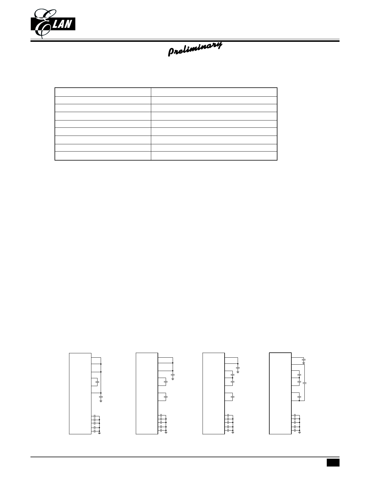
Case of the double step-up, the triple step-up and Case of the quad step-up VOUT is output voltage pin the bias
voltage V1 is supported from VREG.
(a) Double step-up, (b) Triple step-up, (c) Quad step-up (d) five times step-up C1=0.47 to 1.0£gf, C2=1.0 to
4.7uf
VOUT
VSS4
VSS3
CB
CA
VSS2+
VSS2-
VREG
V1
V2
V3
V4
V5
C1
C2
C2
VOUT
VSS4
VSS3
CB
CA
VSS2+
VSS2-
VREG
V1
V2
V3
V4
V5
C2
C2
C2
C1
VOUT
VSS4
VSS3
CB
CA
VSS2+
VSS2-
VREG
V1
V2
V3
V4
V5
C2
C2
C2
C2
C1
VOUT
VSS4
C2
VSS3
CB
CA
C2
C2
C2
VSS2+
C2
VSS2-
VREG
V1
V2 C1
V3
V4
V5
(a) VOUT=2*VDD (b) VOUT=3*VDD (c) VOUT=4*VDD
FIG. 9
* This specification are subject to be changed without notice.
(d) VOUT=5*VDD
9.14.2001 11
11 Page | ||
| Páginas | Total 22 Páginas | |
| PDF Descargar | [ Datasheet EM83040BBQ.PDF ] | |
Hoja de datos destacado
| Número de pieza | Descripción | Fabricantes |
| EM83040BBQ | LCD CONTROLLER | ELAN Microelectronics Corp |
| Número de pieza | Descripción | Fabricantes |
| SLA6805M | High Voltage 3 phase Motor Driver IC. |
Sanken |
| SDC1742 | 12- and 14-Bit Hybrid Synchro / Resolver-to-Digital Converters. |
Analog Devices |
|
DataSheet.es es una pagina web que funciona como un repositorio de manuales o hoja de datos de muchos de los productos más populares, |
| DataSheet.es | 2020 | Privacy Policy | Contacto | Buscar |
