|
|
|
PDF EL5375 Data sheet ( Hoja de datos )
| Número de pieza | EL5375 | |
| Descripción | 550MHz Differential Line Receivers | |
| Fabricantes | Intersil Corporation | |
| Logotipo | ||
Hay una vista previa y un enlace de descarga de EL5375 (archivo pdf) en la parte inferior de esta página. Total 15 Páginas | ||
|
No Preview Available !
®
Data Sheet
EL5175, EL5375
July 9, 2004
FN7306.3
550MHz Differential Line Receivers
The EL5175 and EL5375 are single
and triple high bandwidth amplifiers
designed to extract the difference
signal from noisy environments. They are primarily targeted
for applications such as receiving signals from twisted-pair
lines or any application where common mode noise injection
is likely to occur.
The EL5175 and EL5375 are stable for a gain of one and
requires two external resistors to set the voltage gain for
each channel.
The output common mode level is set by the reference pin
(VREF), which has a -3dB bandwidth of over 450MHz.
Generally, this pin is grounded but it can be tied to any
voltage reference.
The output can deliver a maximum of ±60mA and is short
circuit protected to withstand a temporary overload
condition.
The EL5175 is available in the 8-pin SO and 8-pin MSOP
packages and the EL5375 in the 24-pin QSOP package. All
are specified for operation over the full -40°C to +85°C
temperature range.
Ordering Information
PART
NUMBER
EL5175IS
EL5175IS-T7
EL5175IS-T13
EL5175IY
EL5175IY-T7
EL5175IY-T13
EL5375IU
EL5375IU-T7
EL5375IU-T13
PACKAGE
8-Pin SO
8-Pin SO
8-Pin SO
8-Pin MSOP
8-Pin MSOP
8-Pin MSOP
24-Pin QSOP
24-Pin QSOP
24-Pin QSOP
TAPE &
REEL
-
7”
13”
-
7”
13”
-
7”
13”
PKG. DWG. #
MDP0027
MDP0027
MDP0027
MDP0043
MDP0043
MDP0043
MDP0040
MDP0040
MDP0040
Features
• Differential input range ±2.3V
• 550MHz 3dB bandwidth
• 900V/µs slew rate
• 60mA maximum output current
• Single 5V or dual ±5V supplies
• Low power - 9.6mA per channel
Applications
• Twisted-pair receivers
• Differential line receivers
• VGA over twisted-pair
• ADSL/HDSL receivers
• Differential to single-ended amplification
• Reception of analog signals in a noisy environment
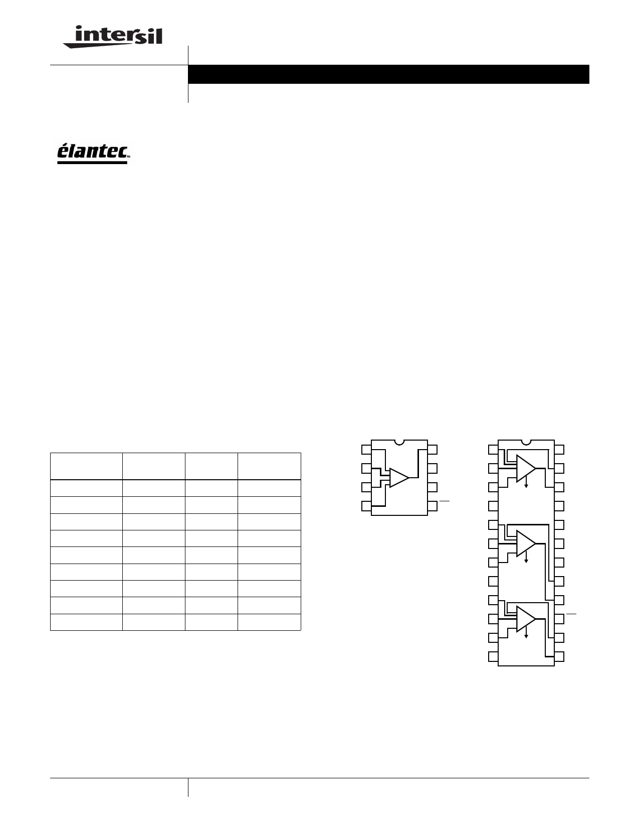
Pinouts
EL5175
(8-PIN SO, MSOP)
TOP VIEW
EL5375
(24-PIN QSOP)
TOP VIEW
FB 1
8 OUT REF1 1
24 NC
IN+ 2
IN- 3
+-
7 VS-
6 VS+
INP1 2
INN1 3
+
-
23 FB1
22 OUT1
REF 4
5 EN
NC 4
21 NC
REF2 5
20 VSP
INP2 6
INN2 7
+
-
19 VSN
18 NC
NC 8
17 FB2
REF3 9
16 OUT2
INP3 10
INN3 11
+
-
15 EN
14 FB3
NC 12
13 OUT3
1 CAUTION: These devices are sensitive to electrostatic discharge; follow proper IC Handling Procedures.
1-888-INTERSIL or 321-724-7143 | Intersil (and design) is a registered trademark of Intersil Americas Inc.
Copyright © Intersil Americas Inc. 2003-2004. All Rights Reserved. Elantec is a registered trademark of Elantec Semiconductor, Inc.
All other trademarks mentioned are the property of their respective owners.
1 page 
Connection Diagrams
RG
RF=0Ω
-5V
1 FB
OUT 8
INP
2 INP
VSN 7
CL
2.7pF
INN
3 INN
VSP 6
REF
4 REF
EN 5
RS2 RS2 RS3
50Ω 50Ω 50Ω
EL5175
+5V
VOUT
RL
500Ω
EN
REF1
INP1
INN1
REF2
INP2
INN2
REF3
INP3
INN3
RSP1 RSN1 RSR1 RSP2 RSN2 RSR2 RSP3 RSN3 RSR3
50Ω 50Ω 50Ω 50Ω 50Ω 50Ω 50Ω 50Ω 50Ω
RG
1 REF1
2 INP1
NC 24
FB1 23
RF
3 INN1 OUT1 22
4 NC
NC 21
5 REF2
VSP 20
6 INP2
7 INN2
8 NC
VSN 19
NC 18
FB2 17
RG
RF
9 REF3
10 INP3
11 INN3
OUT2 16
EN 15
FB3 14
RG
RF
12 NC
OUT3 13
EL5175
+5V
-5V
ENABLE
CL1
2.7pF
CL2
2.7pF
CL3
2.7pF
RL1
500Ω
OUT1
RL2
500Ω
OUT2
RL3
500Ω
OUT3
5 Page 
EL5175, EL5375
120µA for IS- typically, thereby effectively eliminating the
power consumption. The amplifier's power down can be
controlled by standard CMOS signal levels at the ENABLE
pin. The applied logic signal is relative to VS+ pin. Letting the
EN pin float or applying a signal that is less than 1.5V below
VS+ will enable the amplifier. The amplifier will be disabled
when the signal at EN pin is above VS+ - 0.5V. If a TTL
signal is used to control the enabled/disabled function,
Figure 22 could be used to convert the TTL signal to CMOS
signal.
5V
CMOS/TTL
10K
1K
EN
FIGURE 24.
Output Drive Capability
The EL5175 and EL5375 have internal short circuit
protection. Its typical short circuit current is ±67mA. If the
output is shorted indefinitely, the power dissipation could
easily increase such that the part will be destroyed.
Maximum reliability is maintained if the output current never
exceeds ±60mA. This limit is set by the design of the internal
metal interconnections.
Power Dissipation
With the high output drive capability of the EL5175 and
EL5375. It is possible to exceed the 135°C absolute
maximum junction temperature under certain load current
conditions. Therefore, it is important to calculate the
maximum junction temperature for the application to
determine if the load conditions or package types need to be
modified for the amplifier to remain in the safe operating
area.
The maximum power dissipation allowed in a package is
determined according to:
PDMAX
=
T----J---M-----A----X-----–-----T----A---M-----A----X--
ΘJA
• TJMAX = Maximum junction temperature
• TAMAX = Maximum ambient temperature
• θJA = Thermal resistance of the package
Assume the REF pin is tired to GND for VS = ±5V
application, the maximum power dissipation actually
produced by an IC is the total quiescent supply current times
the total power supply voltage, plus the power in the IC due
to the load, or:
For sourcing:
PDMAX =
VS
×
ISMAX
+
(VS+
–
VOUT
)
×
--V-----O----U----T----
RLOAD
×i
For sinking:
PDMAX = [VS × ISMAX + (VOUT – VS- ) × ILOAD ] × i
Where:
• VS = Total supply voltage
• ISMAX = Maximum quiescent supply current per channel
• VOUT = Maximum output voltage of the application
• RLOAD = Load resistance
• ILOAD = Load current
• i = Number of channels
By setting the two PDMAX equations equal to each other, we
can solve the output current and RLOAD to avoid the device
overheat.
Power Supply Bypassing and Printed Circuit
Board Layout
As with any high frequency device, a good printed circuit
board layout is necessary for optimum performance. Lead
lengths should be as sort as possible. The power supply pin
must be well bypassed to reduce the risk of oscillation. For
normal single supply operation, where the VS- pin is
connected to the ground plane, a single 4.7µF tantalum
capacitor in parallel with a 0.1µF ceramic capacitor from VS+
to GND will suffice. This same capacitor combination should
be placed at each supply pin to ground if split supplies are to
be used. In this case, the VS- pin becomes the negative
supply rail.
For good AC performance, parasitic capacitance should be
kept to minimum. Use of wire wound resistors should be
avoided because of their additional series inductance. Use
of sockets should also be avoided if possible. Sockets add
parasitic inductance and capacitance that can result in
compromised performance. Minimizing parasitic capacitance
at the amplifier's inverting input pin is very important. The
feedback resistor should be placed very close to the
inverting input pin. Strip line design techniques are
recommended for the signal traces.
11
11 Page | ||
| Páginas | Total 15 Páginas | |
| PDF Descargar | [ Datasheet EL5375.PDF ] | |
Hoja de datos destacado
| Número de pieza | Descripción | Fabricantes |
| EL5370 | (EL5170 / EL5370) 100MHz Differential Twisted-Pair Drivers | Intersil Corporation |
| EL5371 | 250MHz Differential Twisted-Pair Drivers | Intersil Corporation |
| EL5372 | (EL5172 / EL5372) 250MHz Differential Line Receivers | Intersil Corporation |
| EL5374 | 550MHz Differential Twisted-Pair Drivers | Intersil |
| Número de pieza | Descripción | Fabricantes |
| SLA6805M | High Voltage 3 phase Motor Driver IC. |
Sanken |
| SDC1742 | 12- and 14-Bit Hybrid Synchro / Resolver-to-Digital Converters. |
Analog Devices |
|
DataSheet.es es una pagina web que funciona como un repositorio de manuales o hoja de datos de muchos de los productos más populares, |
| DataSheet.es | 2020 | Privacy Policy | Contacto | Buscar |