|
|
|
PDF ATF16LV8C-15SI Data sheet ( Hoja de datos )
| Número de pieza | ATF16LV8C-15SI | |
| Descripción | High- Performance EE PLD | |
| Fabricantes | ATMEL Corporation | |
| Logotipo | ||
Hay una vista previa y un enlace de descarga de ATF16LV8C-15SI (archivo pdf) en la parte inferior de esta página. Total 10 Páginas | ||
|
No Preview Available !
Features
• 3.0V to 5.5V Operation
• Industry Standard Architecture
– Emulates Many 20-Pin PALs®
– Low Cost Easy-to-Use Software Tools
• High Speed
– 10 ns Maximum Pin-to-Pin Delay
• Ultra-Low Power
– 5 µA (Max.) Pin-Controlled Power Down Mode Option
– Typical 100 nA Standby
• CMOS and TTL Compatible Inputs and Outputs
– I/O Pin Keeper Circuits
• Advanced Flash Technology
– Reprogrammable
– 100% Tested
• High Reliability CMOS Process
– 20 Year Data Retention
– 100 Erase/Write Cycles
– 2,000V ESD Protection
– 200 mA Latchup Immunity
• Commercial and Industrial Temperature Ranges
• Dual-in-Line and Surface Mount Packages in Standard Pinouts
Description
The ATF16LV8C is a high-performance EECMOS Programmable Logic Device that
utilizes Atmel's proven electrically erasable Flash memory technology. Speeds down
to 10 ns and a 5 µA pin-controlled power down mode option are offered. All speed
ranges are specified over the full 3.0V to 5.25V range for industrial and commercial
temperature ranges.
(continued)
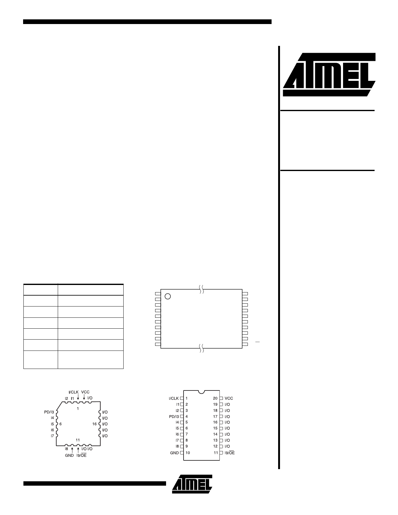
Pin Configurations
TSSOP
Pin Name
CLK
I
I/O
OE
VCC
PD
Function
Clock
Logic Inputs
Bidirectional Buffers
Output Enable
(+3V to 5.5V) Supply
Programmable Power
Down Option
I/CLK
I1
I2
PD/I3
I4
I5
I6
I7
I8
GND
1
2
3
4
5
6
7
8
9
10
20 VCC
19 I/O
18 I/O
17 I/O
16 I/O
15 I/O
14 I/O
13 I/O
12 I/O
11 19/OE
High-
Performance
EE PLD
ATF16LV8C
PLCC
DIP/SOIC
Top View
Rev. 0403E–06/98
1
1 page 
ATF16LV8C
Input Test Waveforms and
Measurement Levels:
tR, tF < 1.5ns (10% to 90%)
Output Test Loads:
Commercial
3.3V
R1 = 316
R2 = 348
OUTPUT
PIN
CL = 35 pF
Note:
Similar devices are tested with slightly different loads.
These load differences may affect output signals’ delay
and slew rate. Atmel devices are tested with sufficient
margins to meet compatible devices.
Pin Capacitance
(f = 1 MHz, T = 25°C)(1)
Typ Max
Units
Conditions
CIN
COUT
Note:
58
pF VIN = 0V
68
pF VOUT = 0V
1. Typical values for nominal supply voltage. This parameter is only sampled and is not 100% tested.
Power Up Reset
The ATF16LV8C’s registers are designed to reset during
power up. At a point delayed slightly from VCC crossing
VRST, all registers will be reset to the low state. As a result,
the registered output state will always be high on power-up.
This feature is critical for state machine initialization. How-
ever, due to the asynchronous nature of reset and the
uncertainty of how VCC actually rises in the system, the fol-
lowing conditions are required:
1. The VCC rise must be monotonic from below 0.7
volts.
2. The signals from which the clock is derived must
remain stable during TPR.
3. After TPR, all input and feedback setup times must
be met before driving the clock term high.
Parameter
TPR
VRST
Description
Power-Up
Reset Time
Power-Up
Reset
Voltage
Typ Max Units
600 1,000
ns
2.5 3.0
V
5
5 Page | ||
| Páginas | Total 10 Páginas | |
| PDF Descargar | [ Datasheet ATF16LV8C-15SI.PDF ] | |
Hoja de datos destacado
| Número de pieza | Descripción | Fabricantes |
| ATF16LV8C-15SC | High- Performance EE PLD | ATMEL Corporation |
| ATF16LV8C-15SI | High- Performance EE PLD | ATMEL Corporation |
| Número de pieza | Descripción | Fabricantes |
| SLA6805M | High Voltage 3 phase Motor Driver IC. |
Sanken |
| SDC1742 | 12- and 14-Bit Hybrid Synchro / Resolver-to-Digital Converters. |
Analog Devices |
|
DataSheet.es es una pagina web que funciona como un repositorio de manuales o hoja de datos de muchos de los productos más populares, |
| DataSheet.es | 2020 | Privacy Policy | Contacto | Buscar |