|
|
|
PDF DS3884 Data sheet ( Hoja de datos )
| Número de pieza | DS3884 | |
| Descripción | Pythagoras Processor | |
| Fabricantes | Mitel Networks Corporation | |
| Logotipo | ||
Hay una vista previa y un enlace de descarga de DS3884 (archivo pdf) en la parte inferior de esta página. Total 12 Páginas | ||
|
No Preview Available !
PDSP16330/A/B
Pythagoras Processor
Supersedes version in December 1993 Digital Video & DSP IC Handbook, HB3923-1
DS3884 - 1.3 September 1996
The PDSP16330 is a high speed digital CMOS IC that
converts Cartesian data (Real and Imaginary) into Polar form
(Magnitude and Phase), at rates up to 20MHz. Cartesian
16+16 bit 2's complement or Sign-Magnitude data is
converted into 16 bit Phase format. The Magnitude output may
be scaled in amplitude by powers of 2. The Phase output
represents a full 2 x π field to eliminate phase ambiguities.
Polyimide is used as an inter-layer dielectric and as
glassivation.
The PDSP16330 is offered in three speed grades: a
basic 10MHz part (PDSP16330), a 20MHz version
(PDSP16330A) and a 25MHz version (PDSP16330). A MIL-
STD-883 version is also detailed in a separate datasheet.
FEATURES
25MHz Cartesian to Polar Conversion
16-Bit Cartesian Inputs
16-Bit Magnitude Output
12-Bit Phase Output
2’s Complement or Sign-Magnitude Input Formats
Three-state Outputs and Independent
Data Enables Simplify System Interfacing
Magnitude Scaling Facility with Overflow Flag
Less than 400 mW Power Dissipation at 10MHz
84-pin PGA or 100 pin QFP Package or 84 LCC
APPLICATIONS
Digital Signal Processing
Digital Radio
Radar Processing
Sonar Processing
Robotics
ASSOCIATED PPODUCTS
PDSP16112 16 X 12 Complex Multiplier
PDSP16116 16 X 16 Complex Multiplier
PDSP16318 Complex Accumulator
PDSP16350 I/Q Splitter and NCO
PDSP16510A Stand Alone FFT Processor
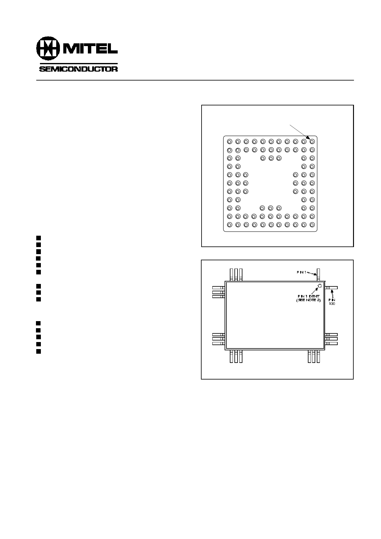
PIN 1A INDEX MARK
ON TOP SURFACE
A
B
C
D
E
F
G
H
J
K
L
11 10 9 8 7 6 5 4 3 2 1
AC84
Fig.1 Pin connections - bottom view (PGA)
GG100/R
Fig.2 Pin connections - QFP Package
1 page 
SWITCHING CHARACTERISTICS
PDSP16330/A/B
Characteristic
Value
PDSP16330 PDSP16330A PDSP16330B
Min. Max. Min. Max. Min. Max.
Units
Conditions
† Input data setup to clock rising edge
15
12
12
ns
† Input data Hold after clock rising edge
2
2
2
ns
† CEX, CEY Setup to clock rising edge
† CEX, CEY Hold aher clock rising edge
30
0
12
0
12
0
ns
ns
† FORM, S1:0 Setup to clock rising edge 15
12
12
ns
† FORM, S1:0 Hold after clock rising edge 7
2
2
ns
† Clock rising edge to valid data
* Clock period
5 40 5 25
100 50
5 25
40
ns 2 x LSTTL + 20pF
ns
† Clock high time
25 15
15
ns
† Clock low time
25 15
15
ns
† Latency
† OEM, OEP low to data high data valid
24 24 24 24
30 25
24 24 cycles
25 ns 2 x LSTTL + 20pF
† OEM, OEP low to data low data valid
30 25 25
ns 2 x LSTTL + 20pF
† OEM, OEP high to data high impedance
30
25 25
ns 2 x LSTTL + 20pF
† OEM, OEP low to data high impedance
30
25 25
ns 2 x LSTTL + 20pF
† Vcc current (TTL input levels)
110 180 225
mA VCC = Max
Outputs unloaded
Clock freq. = Max
† Vcc current (CMOS input levels)
70 120 150
mA VCC = Max
Outputs unloaded
Clock freq. = Max
NOTES
1. LSTTL is equivalent to IOH = 20µA, IOL = -0.4mA
2. Current is defined as negative into the device
3. CMOS input levels are defined as: VIH = VDD - 0.5V, VIL = +0.5V
4. All parameters marked * are tested during production.
Parameters marked † are guaranteed by design and characterisation.
5. All timings are dependent on silicon speed. This speed is tested by measuring clock period.
This guarantees all other timings by characterisation and design.
ABSOLUTE MAXIMUM RATINGS
Supply voltage, Vcc
-0.5V to + 7.0V
Input voltage, V
-0.5V to VCC + 0.5V
IN
Output voltage, V
-0.5V to VCC + 0.5V
our
Clamp diode current per pin, IK (see Note 2)
±18mA
Static discharge voltage (HMB), VSTAT
500V
Storage temperature. Tstg
-65°C to + 150°C
Ambient temperature with
power applied Tamb:
Commercial
0°C to + 70°C
Industrial
-40°C to + 85°C
Military
-55 °C to + 125°C
Package power dissipation PTOT
Junction temperature
1200mW
150°C
THERMAL CHARACTERISTICS
Package Type
θJC°C/W
AC 12
GG 12
θJA°C/W
36
35
NOTES
1. Exceeding these ratings may cause permanent damage.
Functional operatlon under these conditions is not implied.
2. Maximum dissipation or 1 second should not be exceeded;
only one output to be tested at any one time.
3. Exposure to Absoulte Maximum Ratings for extended periods
may affect device reliability.
5
5 Page 
PDSP16330/A/B
11
11 Page | ||
| Páginas | Total 12 Páginas | |
| PDF Descargar | [ Datasheet DS3884.PDF ] | |
Hoja de datos destacado
| Número de pieza | Descripción | Fabricantes |
| DS3882 | Dual-Channel Automotive CCFL Controller | Maxim Integrated Products |
| DS3883 | BTL 9-Bit Data Transceiver | National Semiconductor |
| DS3883A | BTL 9-Bit Data Transceiver | National Semiconductor |
| DS3883A | DS3883A BTL 9-Bit Data Transceiver (Rev. A) | Texas Instruments |
| Número de pieza | Descripción | Fabricantes |
| SLA6805M | High Voltage 3 phase Motor Driver IC. |
Sanken |
| SDC1742 | 12- and 14-Bit Hybrid Synchro / Resolver-to-Digital Converters. |
Analog Devices |
|
DataSheet.es es una pagina web que funciona como un repositorio de manuales o hoja de datos de muchos de los productos más populares, |
| DataSheet.es | 2020 | Privacy Policy | Contacto | Buscar |