|
|
|
PDF DS2430 Data sheet ( Hoja de datos )
| Número de pieza | DS2430 | |
| Descripción | 256-Bit 1-Wire EEPROM | |
| Fabricantes | Dallas Semiconducotr | |
| Logotipo | ||
Hay una vista previa y un enlace de descarga de DS2430 (archivo pdf) en la parte inferior de esta página. Total 16 Páginas | ||
|
No Preview Available !
www.dalsemi.com
DS2430A
256-Bit 1-WireTM EEPROM
FEATURES
§ 256-bit Electrically Erasable Programmable
Read Only Memory (EEPROM) plus 64-bit
one-time programmable application register
§ Unique, factory-lasered and tested 64-bit
registration number (8-bit family code + 48-bit
serial number + 8-bit CRC tester) assures
absolute identity because no two parts are alike
§ Built-in multidrop controller ensures
compatibility with other MicroLAN products
§ EEPROM organized as one page of 32 bytes
for random access
§ Reduces control, address, data and power to a
single data pin
§ Directly connects to a single port pin of a
microprocessor and communicates at up to
16.3 kbits per second
§ 8-bit family code specifies DS2430A
communication requirements to reader
§ Presence detector acknowledges when reader
first applies voltage
§ Low cost TO-92 or 6-pin TSOC surface mount
package
§ Reads and writes over a wide voltage range of
2.8V to 6.0V from -40°C to +85°C
ORDERING INFORMATION
DS2430A TO-92 package
DS2430AP 6-pin TSOC package
DS2430AT Tape & Reel version of DS2430A
DS2430AV Tape & Reel version of DS2430AP
DS2430AX Chip Scale Pkg., Tape & Reel
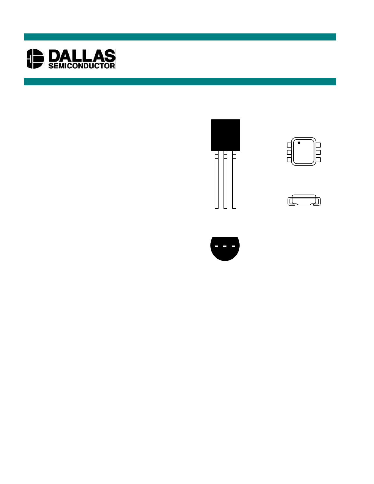
PIN ASSIGNMENT
TO-92
DALLAS
DS2430A
TSOC PACKAGE
16
25
34
TOP VIEW
3.7 X 4.0 X 1.5 mm
123
12 3
BOTTOM VIEW
See Mech.
Drawings Section
SIDE VIEW
See Mech.
Drawing Section
PIN DESCRIPTION
TO-92 TSOC
Pin 1 Ground Ground
Pin 2 Data
Data
Pin 3 NC
NC
Pin 4 ––––
NC
Pin 5 ––––
NC
Pin 6 ––––
1 of 16
102199
1 page 
DS2430A
MEMORY
The memory of the DS2430A consists of three separate sections, called data memory, application register
and status register (Figure 5). The data memory and the application register each has its own intermediate
storage area called scratchpad that acts as a buffer when writing to the device. The data memory can be
read and written as often as desired. The application register, however, is one-time programmable only.
Once the application register is programmed, it is automatically write protected. The status register will
indicate if the application register is already locked or if it is still available for storing data. As long as the
application register is unprogrammed, the status register will read FFh. Copying data from the register
scratchpad to the application register will clear the 2 least significant bits of the status register, yielding a
FCh the next time one reads the status register.
DS2430A MEMORY MAP Figure 5
MEMORY FUNCTION COMMANDS
The “Memory Function Flow Chart” (Figure 6) describes the protocols necessary for accessing the
different memory sections of the DS2430A. An example is shown later in this document.
WRITE SCRATCHPAD [0Fh]
After issuing the Write Scratchpad command, the master must first provide a 1-byte address, followed by
the data to be written to the scratchpad for the data memory. The DS2430A will automatically increment
the address after every byte it received. After having received a data byte for address 1Fh, the address
counter will wrap around to 00h for the next byte and writing continues until the master sends a reset
pulse.
READ SCRATCHPAD [AAh]
This command is used to verify data previously written to the scratchpad before it is copied into the final
storage EEPROM memory. After issuing the Read Scratchpad command, the master must provide the 1-
byte starting address from where data is to be read. The DS2430A will automatically increment the
address after every byte read by the master. After the data of address 1Fh has been read, the address
counter will wrap around to 00h for the next byte and reading continues until the master sends a reset
pulse.
5 of 16
102199
5 Page 
Transaction Sequence
The sequence for accessing the DS2430A via the 1-Wire port is as follows:
§ Initialization
§ ROM Function Command
§ Memory Function Command
§ Transaction/Data
DS2430A
INITIALIZATION
All transactions on the 1-Wire bus begin with an initialization sequence. The initialization sequence
consists of a reset pulse transmitted by the bus master followed by a presence pulse(s) transmitted by the
slave(s).
The presence pulse lets the bus master know that the DS2430A is on the bus and is ready to operate. For
more details, see the “1-Wire Signaling” section.
ROM FUNCTION COMMANDS
Once the bus master has detected a presence, it can issue one of the four ROM function commands. All
ROM function commands are 8 bits long. A list of these commands follows (refer to flowchart in Figure
8):
Read ROM [33h]
This command allows the bus master to read the DS2430A’s 8-bit family code, unique 48-bit serial
number, and 8-bit CRC. This command can be used only if there is a single DS2430A on the bus. If more
than one slave is present on the bus, a data collision will occur when all slaves try to transmit at the same
time (open drain will produce a wired-AND result). The resultant family code and 48-bit serial number
will usually result in a mismatch of the CRC.
Match ROM [55h]
The Match ROM command, followed by a 64-bit ROM sequence, allows the bus master to address a
specific DS2430A on a multidrop bus. Only the DS2430A that exactly matches the 64-bit ROM sequence
will respond to the subsequent memory function command. All slaves that do not match the 64-bit ROM
sequence will wait for a reset pulse. This command can be used with a single or multiple devices on the
bus.
Skip ROM [CCh]
This command can save time in a single-drop bus system by allowing the bus master to access the
memory functions without providing the 64-bit ROM code. If more than one slave is present on the bus
and a read command is issued following the Skip ROM command, data collision will occur on the bus as
multiple slaves transmit simultaneously (open drain pulldowns will produce a wired-AND result).
Search ROM [F0h]
When a system is initially brought up, the bus master might not know the number of devices on the 1-
Wire bus or their 64-bit ROM codes. The Search ROM command allows the bus master to use a process
of elimination to identify the 64-bit ROM codes of all slave devices on the bus. The Search ROM process
is the repetition of a simple, three-step routine: read a bit, read the complement of the bit, then write the
desired value of that bit. The bus master performs this simple, three-step routine on each bit of the ROM.
11 of 16
102199
11 Page | ||
| Páginas | Total 16 Páginas | |
| PDF Descargar | [ Datasheet DS2430.PDF ] | |
Hoja de datos destacado
| Número de pieza | Descripción | Fabricantes |
| DS2430 | 256-Bit 1-Wire EEPROM | Dallas Semiconducotr |
| DS2430A | 256-Bit 1-Wire EEPROM | Maxim Integrated |
| DS2431 | 1024-Bit 1-Wire EEPROM | Dallas Semiconducotr |
| DS2431 | 1-Wire EEPROM | Maxim Integrated |
| Número de pieza | Descripción | Fabricantes |
| SLA6805M | High Voltage 3 phase Motor Driver IC. |
Sanken |
| SDC1742 | 12- and 14-Bit Hybrid Synchro / Resolver-to-Digital Converters. |
Analog Devices |
|
DataSheet.es es una pagina web que funciona como un repositorio de manuales o hoja de datos de muchos de los productos más populares, |
| DataSheet.es | 2020 | Privacy Policy | Contacto | Buscar |