|
|
|
PDF DS2196LN Data sheet ( Hoja de datos )
| Número de pieza | DS2196LN | |
| Descripción | T1 Dual Framer LIU | |
| Fabricantes | Dallas Semiconducotr | |
| Logotipo | ||
Hay una vista previa y un enlace de descarga de DS2196LN (archivo pdf) en la parte inferior de esta página. Total 30 Páginas | ||
|
No Preview Available !
www.maxim-ic.com
GENERAL DESCRIPTION
The DS2196 T1 dual framer LIU is designed for T1
transmission equipment. The DS2196 combines dual
optimized framers together with a LIU. This
combination allows the users to extract and insert
facility data-link (FDL) messages in the receive and
transmit paths, collect line performance data, and
perform basic channel conditioning and maintenance.
The DS2196 contains all of the necessary functions
for connection to T1 lines whether they are DS1 long
haul or DSX–1 short haul. The clock recovery
circuitry automatically adjusts to T1 lines from 0ft to
over 6000ft in length. The device can generate both
DSX–1 line buildouts as well as CSU line buildouts
of -7.5dB, -15dB, and -22.5dB. The on-board jitter
attenuator (selectable to either 32 bits or 128 bits) can
be placed in either the transmit or receive data paths.
The framer locates the frame and multiframe
boundaries and monitors the data stream for alarms.
The device contains a set of internal registers that the
user can access and use to control the unit’s operation
of the unit. Quick access through the parallel control
port allows a single controller to handle many T1
lines. The device fully meets all of the latest T1
specifications.
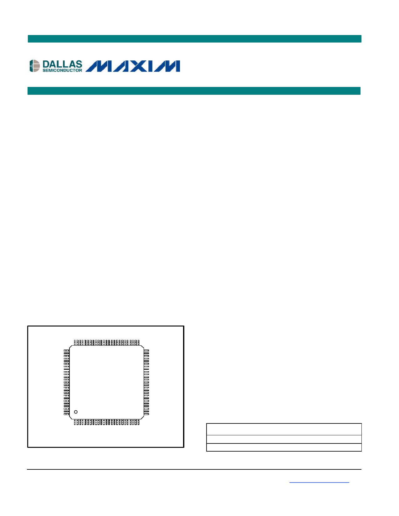
PACKAGE OUTLINE
DS2196
100
1
DS2196
T1 Dual Framer LIU
FEATURES
§ Two full-featured framers and a short/long-haul
line interface unit (LIU) in one small package
§ Based on Dallas Semiconductor’s single -chip
transceiver (SCT) family
§ Two HDLC controllers with 64-byte buffers that
can be used for the FDL or DS0 channels
§ Supports NPRMs and SPRMs as per ANSI
T1.403-1998
§ Can be combined with a short/long-haul LIU or a
HDSL modem chipset to create a low-cost office
repeater/NIU/CSU, or a HDSL1/HDSL2 terminal
unit with enhanced monitoring and data link
control
§ Supports fractional T1
§ Can convert from D4 to ESF framing and ESF to
D4 framing
§ 32-bit or 128-bit crystal-less jitter attenuator
§ Can generate and detect repeating in-band
patterns from 1 to 8 bits or 16 bits in length
§ Detects and generates RAI-CI and AIS-CI
§ Generates DS1 idle codes
§ On-chip programmable BERT generator and
detector
§ All key signals are routed to pins to support
numerous hardware configurations
§ Supports both NRZ and bipolar interfaces
§ Can create errors in the F-bit position and BERT
interface data paths
§ 8-bit parallel control port that can be used
directly on either multiplexed or nonmultiplexed
buses (Intel or Motorola)
§ IEEE 1149.1 JTAG Boundary Scan
§ 3.3V supply with 5V tolerant inputs and outputs
§ 100-pin LQFP (14 mm x 14 mm) package
ORDERING INFORMATION
PART TEMP RANGE PIN-PACKAGE
DS2196L
DS2196LN
0ºC to +70ºC 100 LQFP
-40ºC to +85ºC 100 LQFP
Note: Some revisions of this device may incorporate deviations from published specifications known as errata. Multiple revisions of any device
may be simultaneously available through various sales channels. For information about device errata, click here: www.maxim-ic.com/errata.
1 of 157
093002
1 page 
LIST OF TABLES
DS2196
Table 2-1: Pin Description Sorted by Pin Number................................................................................ 10
Table 4-1: Register Map Sorted by Address .......................................................................................... 21
Table 6-1: Output Pin Test Modes .......................................................................................................... 36
Table 6-2: Receive Data Source Mux Modes......................................................................................... 37
Table 6-3: TPOSB/TNEGB Data Source Select..................................................................................... 38
Table 7-1: Receive T1 Level Indication .................................................................................................. 57
Table 7-2: Alarm Criteria ........................................................................................................................ 59
Table 8-1: Line Code Violation Counting Arrangements..................................................................... 66
Table 8-2: Path Code Violation Counting Arrangements..................................................................... 67
Table 8-3: Multiframes Out Of Sync Counting Arrangements............................................................ 67
Table 12-1: Transmit Code Length......................................................................................................... 75
Table 12-2: Receive Code Length ........................................................................................................... 75
Table 15-1: Bert Pattern Select Options ................................................................................................. 89
Table 15-2: Repetitive Pattern Length Options ..................................................................................... 90
Table 15-3: Bert Rate Insertion Select.................................................................................................... 91
Table 16-1: Error Rate Options .............................................................................................................. 98
Table 16-2: Error Insertion examples..................................................................................................... 99
Table 17-1: Transmit HDLC Configuration .......................................................................................... 99
Table 18-1: HDLC/BOC Controller Register List............................................................................... 102
Table 19-1: Line Build Out Select In LICR ......................................................................................... 119
Table 19-2: Transformer Specifications ............................................................................................... 120
Table 20-1: Instruction Codes For The DS21352/552 IEEE 1149.1 Architecture ............................ 128
Table 20-2: ID Code Structure .............................................................................................................. 128
Table 20-3: Device ID Codes.................................................................................................................. 129
Table 20-4: Boundary Scan Register Description................................................................................ 130
5 of 157
5 Page 
PIN SYMBOL
43 TCLKOB
44 DVSS
45 DVDD
46 TCLKOA
47 TNEGOA /
TFSYNCA
48 TPOSOA /
TNRZA
49 TSERA
50 TCLKA
51 TSYNCA
52 TCHCLKA /
TLCLKA
53 TCHBLKA /
TLINKA
54 MUX
55 D0 / AD0
56 D1 / AD1
57 D2 / AD2
58 D3 / AD3
59 D4 / AD4
60 D5 / AD5
61 D6 / AD6
62 D7 / AD7
63 DVSS
64 DVDD
65 A0
66 A1
67 A2
68 A3
69 A4
70 A5
71 A6
72 A7 / ALE(AS)
73 RD*(DS*)
74 CS*
75 WR*(R/W*)
76 RCHBLKA /
RLINKA
77 RCHCLKA /
RLCLKA
78 RCLKIA
79 RPOSIA
80 RNEGIA
81 RCLKA
82 RSERA
83 RMSYNCA
84 RFSYNCA
85 RLOSA/
LOTCA
TYPE
O
–
–
O
O
O
I
I
I/O
O
I/O
I
I/O
I/O
I/O
I/O
I/O
I/O
I/O
I/O
–
–
I
I
I
I
I
I
I
I
I
I
I
O
O
I
I
I
O
O
O
O
O
DS2196
FUNCTION
Transmit Clock Output from Formatter B.
Digital Signal Ground.
Digital Positive Supply. 3.3V (±5%).
Transmit Clock Output from Formatter A.
Transmit Negative Data Output from Formatter A /
Transmit Frame Sync Pulse Output from Formatter A.
Transmit Positive Data Output / Transmit NRZ Data Output from
Formatter A.
Transmit Serial Data Input for Formatter A.
Transmit Clock Input for Formatter A.
Transmit Frame & Multiframe Pulse for/from Formatter A.
Transmit DS0 Channel Clock Output from Formatter A /
Transmit FDL Link Clock Output from Formatter A.
Transmit Channel Blocking Clock Output from Formatter A /
Transmit FDL Link Data Input for Formatter A.
Bus Operation. 0 = Non-Mux Bus / 1 = Mux Bus Operation.
Data Bus Bit 0 / Address/Data Bus Bit 0. LSB.
Data Bus Bit 1 / Address/Data Bus Bit 1.
Data Bus Bit 2 / Address/Data Bus Bit 2.
Data Bus Bit 3 / Address/Data Bus Bit 3.
Data Bus Bit 4 / Address/Data Bus Bit 4.
Data Bus Bit 5 / Address/Data Bus Bit 5.
Data Bus Bit 6 / Address/Data Bus Bit 6.
Data Bus Bit 7 / Address/Data Bus Bit 7. MSB.
I/O Digital Signal Ground.
I/O Digital Positive Supply. 3.3V (±5%).
Address Bus Bit 0. LSB.
Address Bus Bit 1
Address Bus Bit 2
Address Bus Bit 3
Address Bus Bit 4
Address Bus Bit 5
Address Bus Bit 6
Address Bus Bit 7 / Address Latch Enable (Address Strobe). MSB.
Read Input (Data Strobe).
Chip Select. Active Low Signal.
Write Input (Read/Write).
Receive Channel Blocking Clock Output from Framer A /
Receive FDL Link Data Output from Framer A.
Receive DS0 Channel Clock Output from Framer A /
Receive FDL Link Clock Output from Framer A.
Receive Clock Input for Framer A.
Receive Positive & NRZ Data Input for Framer A.
Receive Negative & NRZ Data Input for Framer A.
Receive Clock Output from Framer A.
Receive Serial Data Output from Framer A.
Receive Multiframe Pulse from Framer A.
Receive Frame Pulse from Framer A.
Receive Loss Of Synchronization from Framer A /
Loss of Transmit Clock Framer A.
11 of 157
11 Page | ||
| Páginas | Total 30 Páginas | |
| PDF Descargar | [ Datasheet DS2196LN.PDF ] | |
Hoja de datos destacado
| Número de pieza | Descripción | Fabricantes |
| DS2196L | T1 Dual Framer LIU | Dallas Semiconducotr |
| DS2196LN | T1 Dual Framer LIU | Dallas Semiconducotr |
| Número de pieza | Descripción | Fabricantes |
| SLA6805M | High Voltage 3 phase Motor Driver IC. |
Sanken |
| SDC1742 | 12- and 14-Bit Hybrid Synchro / Resolver-to-Digital Converters. |
Analog Devices |
|
DataSheet.es es una pagina web que funciona como un repositorio de manuales o hoja de datos de muchos de los productos más populares, |
| DataSheet.es | 2020 | Privacy Policy | Contacto | Buscar |