|
|
PDF DS2188 Data sheet ( Hoja de datos )
| Número de pieza | DS2188 | |
| Descripción | T1/CEPT Jitter Attenuator | |
| Fabricantes | Dallas Semiconducotr | |
| Logotipo | ||
Hay una vista previa y un enlace de descarga de DS2188 (archivo pdf) en la parte inferior de esta página. Total 11 Páginas | ||
|
No Preview Available !
www.dalsemi.com
FEATURES
§ Attenuates clock and data jitter present in T1
or CEPT lines
§ Meets the jitter attenuation templates
outlined in TR62411, TR-TSY-000170,
G.735, and G.742
§ Only one external component required; either
a 6.176 MHz (T1) or 8.192 MHz (CEPT)
crystal
§ Selectable buffer size of 128 or 32 bits
§ Jitter attenuation is easily disabled
§ Single +5V supply; low-power CMOS
technology
§ Available in 16-pin DIP and 16-pin SOIC
(DS2188S)
§ Companion to the DS2186 Transmit Line
and DS2187 Receive Line Interface
DS2188
T1/CEPT Jitter Attenuator
PIN ASSIGNMENT
DJA
RPOS
RNEG
RCLK
BDS
TEST
XTAL OUT
VSS
1
2
3
4
5
6
7
8
16 VDD
15 RRPOS
14 RRNEG
13 RRCLK
12 RST
11 BL
10 XTAL2
9 XTAL1
16-Pin DIP/SOIC
DESCRIPTION
The DS2188 T1/CEPT Jitter Attenuator Chip contains a 128 X 2-bit buffer which, in conjunction with an
external 4X crystal, is used to attenuate the incoming jitter present in clock and data. The device meets all
of the latest applicable specifications including those outlined in TR 62411 (Accunet* T1.5 Service
Description and Interface Specifications, December 1990), TR-TSY-000170 (Digital Cross-Connect
System Requirements and Objectives, November 1985), and the CCITT Recommendations G.735 and
G.742. The DS2188 is compatible with the DS2180A T1/ISDN Primary Rate Transceiver and DS2181A
CEPT Transceiver and is the companion to the DS2187 T1/CEPT Receive Line Interface and DS2186
T1/CEPT Transmit Line Interface. It can also be used in conjunction with the DS2190 T1 Network
Interface Unit.
OVERVIEW
The RCLK input is fed to a 128 x 2-bit FIFO where it drives the write pointer for the positive (RPOS) and
negative (RNEG) data. The read pointer of the FIFO and RRCLK is generated by dividing the frequency
of the crystal connected to XTAL1 and XTAL2 by four. The frequency of the crystal is adjusted by a
DPLL to the long-term average frequency of RCLK. As long as the jitter present at RCLK is less than
120 unit intervals peak-to-peak (UIpp), then the FIFO buffer will be able to absorb the incoming jitter and
it will be attenuated in accordance with TR 62411 (December 1990). In this situation, the BL (Buffer
Limit) pin will remain low. Figures 1 and 2 illustrate the DS2188 Jitter Attenuator performance.
1 of 11
092299
1 page 
PIN DESCRIPTION Table 1
DS2188
PIN SYMBOL
1 DJA
2 RPOS
3 RNEG
4 RCLK
5 BDS
6 TEST
7 XTAL OUT
8 VSS
9 XTAL1
10 XTAL2
11 BL
12 RST
13 RRCLK
14 RRNEG
15 RRPOS
16 VDD
TYPE
I
I
I
I
I
I
O
-
I
O
O
I
O
O
O
-
DESCRIPTION
Disable Jitter Attenuation. When high, jittered data and clock at
RPOS, RNEG, and RCLK are passed directly to RRPOS,
RRNEG, and RRCLK.
Receive Positive Data Input. Jittered data input. Sampled on the
falling edge of RCLK.
Receive Negative Data Input. Jittered data input. Sampled on
the falling edge of RCLK.
Receive Clock Input. Jittered input 1.544 MHz or 2.048 MHz
clock.
Buffer Depth Select.
0 = 128 bits
1 = 32 bits
Test Input. In normal applications, this pin should be tied low.
When tied high, used to verify free running frequency of XTAL.
Crystal Frequency Output. Buffered output of the 4X crystal connected
to XTAL1 and XTAL2.
Ground. 0.0 volts.
Crystal Connections. In T1 environments, connect a 6.176 MHz
crystal to these pins. In CEPT environments, connect a 8.192 MHz
crystal to these pins.
Buffer Limit. Transitions high when the buffer fills or empties to
within either 4 bits (BDS=0) or 2 bits (BDS=1) of its capacity. Indicates
that the jitter at RCLK is greater than 120 UIpp (BDS=0) or
28 UIpp (BDS=1).
Reset. Negative-edge triggered; a high-low transition will recenter
the buffer. Activation of this pin may corrupt data through the
DS2188.
Receive Reference Clock. Dejittered 1.544 MHz or 2.048 MHz
clock.
Receive Reference Negative Data Output. Dejittered data output.
Updated on the rising edge of RRCLK.
Receive Reference Positive Data Output. Dejittered data output.
Updated on the rising edge of RRCLK.
Positive Supply. 5.0 volts.
5 of 11
5 Page 
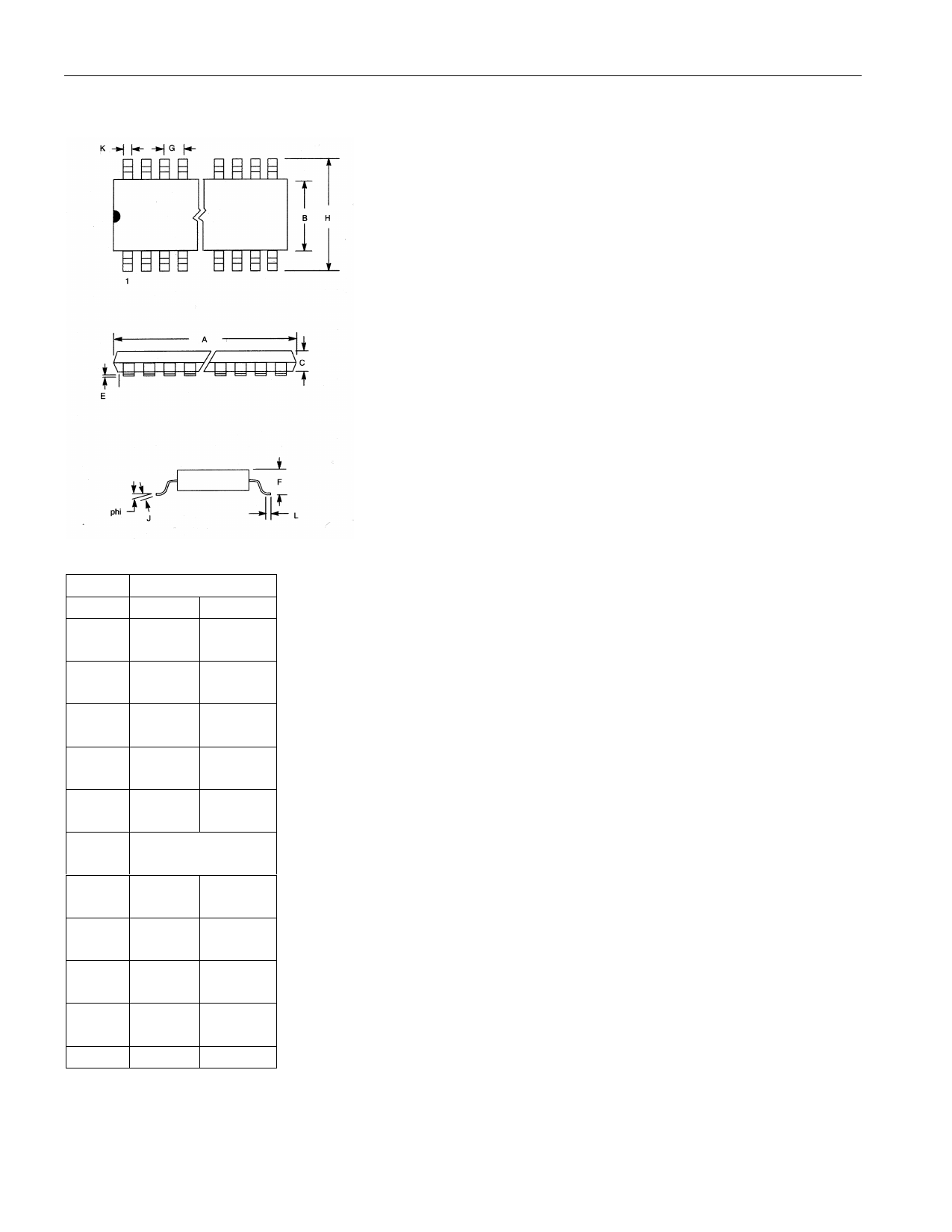
DS1288S T1/CEPT JITTER ATTENTUATOR 16-PIN SOIC
DS2188
PKG
DIM
AIN
MM
B IN
MM
C IN
MM
E IN
MM
F IN
MM
G IN
MM
H IN
MM
J IN
MM
K IN
MM
L IN
MM
phi
16-PIN
MIN MAX
0.402 0.412
10.21 10.46
0.290 0.300
7.37 7.65
0.089 0.095
2.26 2.41
0.004 0.012
0.102
0.30
0.094 0.105
2.38 2.68
0.050 BSC
1.27 BSC
0.398 0.416
10.11 10.57
0.009 0.013
0.229
0.33
0.013 0.019
0.33 0.48
0.016
0.40
0.40 1.02
0° 8°
11 of 11
11 Page | ||
| Páginas | Total 11 Páginas | |
| PDF Descargar | [ Datasheet DS2188.PDF ] | |
Hoja de datos destacado
| Número de pieza | Descripción | Fabricantes |
| DS2180A | T1 Transceiver | Dallas Semiconducotr |
| DS2181A | CEPT Primary Rate Transceiver | Dallas Semiconducotr |
| DS2182 | T1 Line Monitor | Dallas Semiconducotr |
| DS2182A | T1 Line Monitor | Dallas Semiconducotr |
| Número de pieza | Descripción | Fabricantes |
| SLA6805M | High Voltage 3 phase Motor Driver IC. |
Sanken |
| SDC1742 | 12- and 14-Bit Hybrid Synchro / Resolver-to-Digital Converters. |
Analog Devices |
|
DataSheet.es es una pagina web que funciona como un repositorio de manuales o hoja de datos de muchos de los productos más populares, |
| DataSheet.es | 2020 | Privacy Policy | Contacto | Buscar |
