|
|
|
PDF FDC6322 Data sheet ( Hoja de datos )
| Número de pieza | FDC6322 | |
| Descripción | Dual N & P Channel / Digital FET | |
| Fabricantes | Fairchild Semiconductor | |
| Logotipo | ||
Hay una vista previa y un enlace de descarga de FDC6322 (archivo pdf) en la parte inferior de esta página. Total 7 Páginas | ||
|
No Preview Available !
November 1997
FDC6322C
Dual N & P Channel , Digital FET
General Description
These dual N & P Channel logic level enhancement mode field
effec transistors are produced using Fairchild's proprietary,
high cell density, DMOS technology. This very high density
process is especially tailored to minimize on-state resistance.
The device is an improved design especially for low voltage
applications as a replacement for bipolar digital transistors in
load switching applications. Since bias resistors are not
required, this dual digital FET can replace several digital
transistors with difference bias resistors.
Features
N-Ch 25 V, 0.22 A, RDS(ON) = 5 Ω @ VGS= 2.7 V.
P-Ch 25 V, -0.46 A, RDS(ON) = 1.5 Ω @ VGS= -2.7 V.
Very low level gate drive requirements allowing direct
operation in 3 V circuits. VGS(th) < 1.5 V.
Gate-Source Zener for ESD ruggedness.
>6kV Human Body Model
Replace NPN & PNP digital transistors.
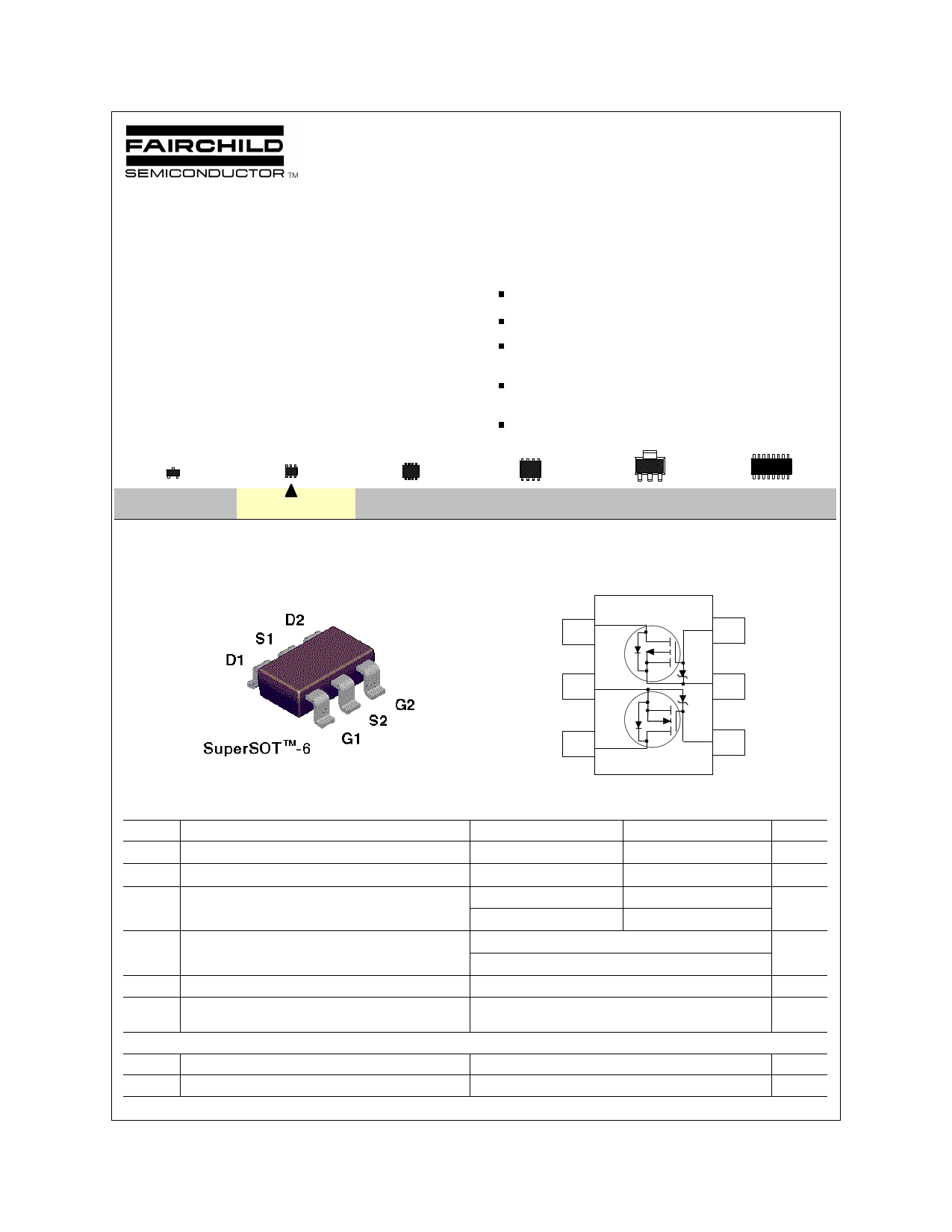
SOT-23
SuperSOTTM-6
Mark: .322
SuperSOTTM-8
SO-8
SOT-223
SOIC-16
43
52
61
Absolute Maximum Ratings TA = 25oC unless other wise noted
Symbol Parameter
N-Channel
VDSS, VCC
VGSS, VIN
ID, IO
Drain-Source Voltage, Power Supply Voltage
Gate-Source Voltage,
Drain/Output Current - Continuous
- Pulsed
25
8
0.22
0.5
PD Maximum Power Dissipation
(Note 1a)
(Note 1b)
TJ,TSTG
ESD
Operating and Storage Tempature Ranger
Electrostatic Discharge Rating MIL-STD-883D
Human Body Model (100pf / 1500 Ohm)
THERMAL CHARACTERISTICS
RθJA
Thermal Resistance, Junction-to-Ambient (Note 1a)
RθJC
Thermal Resistance, Junction-to-Case
(Note 1)
0.9
0.7
-55 to 150
6
140
60
P-Channel
-25
-8
-0.46
-1
Units
V
V
A
W
°C
kV
°C/W
°C/W
© 1997 Fairchild Semiconductor Corporation
FDC6322C.Rev B1
1 page 
Typical Electrical Characteristics: N-Channel (continued)
30
20
10 Ciss
C oss
5
3
2 f = 1 MHz
VGS = 0V
C rss
1
0.1
0.5 1
2
5 10
VDS , DRAIN TO SOURCE VOLTAGE (V)
25
Figure 7. Capacitance Characteristics.
5
ID = 0.2A
4
3
2
1
0
0 0.1
VDS = 5V
10V
15V
0.2 0.3 0.4 0.5 0.6
Q g , GATE CHARGE (nC)
Figure 8. Gate Charge Characteristics.
1
0.5
0.2 RDS(ON) LIMIT
10m1ms s
100ms
0.1
0.05 VGS = 2.7V
SINGLE PULSE
1s
DC
0.02 RθJA =See note 1b
TA = 25°C
0.01
0.5
1
2
5 10 15 25 35
VDS, DRAI N-SOURCE VOLTAGE (V)
Figure 9. Maximum Safe Operating Area.
5
4 SINGLE PULSE
RθJA =See note 1b
TA = 25°C
3
2
1
0
0.01
0.1 1 10
SINGLE PULSE TIME (SEC)
100 300
Figure 10. Single Pulse Maximum Power
Dissipation.
FDC6322C.Rev B1
5 Page | ||
| Páginas | Total 7 Páginas | |
| PDF Descargar | [ Datasheet FDC6322.PDF ] | |
Hoja de datos destacado
| Número de pieza | Descripción | Fabricantes |
| FDC6320 | Dual N & P Channel / Digital FET | Fairchild Semiconductor |
| FDC6320C | Dual N & P Channel / Digital FET | Fairchild Semiconductor |
| FDC6321C | Dual N & P Channel / Digital FET | Fairchild Semiconductor |
| FDC6322 | Dual N & P Channel / Digital FET | Fairchild Semiconductor |
| Número de pieza | Descripción | Fabricantes |
| SLA6805M | High Voltage 3 phase Motor Driver IC. |
Sanken |
| SDC1742 | 12- and 14-Bit Hybrid Synchro / Resolver-to-Digital Converters. |
Analog Devices |
|
DataSheet.es es una pagina web que funciona como un repositorio de manuales o hoja de datos de muchos de los productos más populares, |
| DataSheet.es | 2020 | Privacy Policy | Contacto | Buscar |