|
|
|
PDF DAC7611 Data sheet ( Hoja de datos )
| Número de pieza | DAC7611 | |
| Descripción | 12-Bit Serial Input DIGITAL-TO-ANALOG CONVERTER | |
| Fabricantes | Burr-Brown Corporation | |
| Logotipo | ||
Hay una vista previa y un enlace de descarga de DAC7611 (archivo pdf) en la parte inferior de esta página. Total 12 Páginas | ||
|
No Preview Available !
® DAC7611
DAC7611
DAC7611
12-Bit Serial Input
DIGITAL-TO-ANALOG CONVERTER
FEATURES
q LOW POWER: 2.5mW
q FAST SETTLING: 7µs to 1 LSB
q 1mV LSB WITH 4.095V FULL-SCALE
RANGE
q COMPLETE WITH REFERENCE
q 12-BIT LINEARITY AND MONOTONICITY
OVER INDUSTRIAL TEMP RANGE
q ASYNCHRONOUS RESET TO 0V
q 3-WIRE INTERFACE: Up to 20MHz Clock
q ALTERNATE SOURCE TO DAC8512
APPLICATIONS
q PROCESS CONTROL
q DATA ACQUISITION SYSTEMS
q CLOSED-LOOP SERVO-CONTROL
q PC PERIPHERALS
q PORTABLE INSTRUMENTATION
DESCRIPTION
The DAC7611 is a 12-bit digital-to-analog converter
(DAC) with guaranteed 12-bit monotonicity perfor-
mance over the industrial temperature range. It re-
quires a single +5V supply and contains an input shift
register, latch, 2.435V reference, DAC, and high speed
rail-to-rail output amplifier. For a full-scale step, the
output will settle to 1 LSB within 7µs. The device
consumes 2.5mW (0.5mA at 5V).
The synchronous serial interface is compatible with a
wide variety of DSPs and microcontrollers. Clock
(CLK), serial data in (SDI), and load strobe (LD)
comprise the serial interface. In addition, two control
pins provide a chip select (CS) function and an asyn-
chronous clear (CLR) input. The CLR input can be
used to ensure that the DAC7611 output is 0V on
power-up or as required by the application.
The DAC7611 is available in an 8-lead SOIC or 8-pin
plastic DIP package and is fully specified over the
industrial temperature range of –40°C to +85°C.
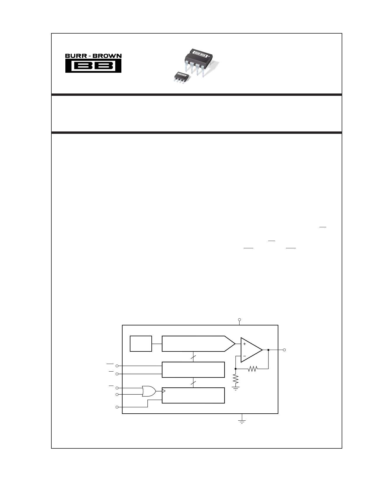
VDD
DAC7611
CLR
LD
CS
CLK
SDI
Ref
12-Bit DAC
12
DAC Register
12
Serial Shift Register
VOUT
GND
International Airport Industrial Park • Mailing Address: PO Box 11400, Tucson, AZ 85734 • Street Address: 6730 S. Tucson Blvd., Tucson, AZ 85706 • Tel: (520) 746-1111 • Twx: 910-952-1111
Internet: http://www.burr-brown.com/ • FAXLine: (800) 548-6133 (US/Canada Only) • Cable: BBRCORP • Telex: 066-6491 • FAX: (520) 889-1510 • Immediate Product Info: (800) 548-6132
© 1997 Burr-Brown Corporation
PDS-11402A
DAPrCinte7d6in1U.1S.A. April, 1998
®
1 page 
TIMING DIAGRAMS
SDI
CLK
CS
LD
(MSB)
(LSB)
D11 D10 D9 D8 D7 D6 D5 D4 D3 D2 D1 D0
tLD1
tCSS
tCSH
tLD2
SDI
CLK
tDS
tCL
tDH
tCH
LD
CLR
FS
VOUT
ZS
tLDW
tS
±1 LSB
Error Band
tCLRW
tS
LOGIC TRUTH TABLE
CS(1) CLK(1) CLR LD
SERIAL SHIFT
REGISTER
DAC REGISTER
HX
LL
LH
L↑
↑L
H(2) X
H(2) X
HX
HX
H H No Change
No Change
H H No Change
No Change
H H No Change
No Change
H H Advanced One Bit No Change
H H Advanced One Bit No Change
H ↓ No Change
Changes to Value of
Serial Shift Register
H L(3) No Change
Transparent
L X No Change
↑ H No Change
Loaded with 000H
Latched with 000H
↑ Positive Logic Transition; ↓ Negative Logic Transition; X = Don’t Care.
NOTES: (1) CS and CLK are interchangeable. (2) A HIGH value is suggested
in order to avoid to “false clock” from advancing the shift register and changing
the DAC voltage. (3) If data is clocked into the serial register while LD is LOW,
the DAC output voltage will change, reflecting the current value of the serial
shift register.
TIMING SPECIFICATIONS
TA = –40°C to +85°C and VDD = +5V.
SYMBOL
DESCRIPTION
MIN TYP MAX UNITS
tCH
tCL
tLDW
tDS
tDH
tCLRW
tLD1
tLD2
tCSS
tCSH
Clock Width HIGH
Clock Width LOW
Load Pulse Width
Data Setup
Data Hold
Clear Pulse Width
Load Setup
Load Hold
Select
Deselect
30
30
20
15
15
30
15
10
30
20
ns
ns
ns
ns
ns
ns
ns
ns
ns
ns
NOTE: All input control signals are specified with tR = tF = 5ns (10% to 90%
of +5V) and timed from a voltage level of 1.6V. These parameters are
guaranteed by design and are not subject to production testing.
®
5 DAC7611
5 Page 
The output amplifier has a 7µs typical settling time to ±1
LSB of the final value. Note that there are differences in the
settling time for negative-going signals versus positive-
going signals.
The rail-to-rail output stage of the amplifier provides the
full-scale range of 0V to 4.095V while operating on a supply
voltage as low as 4.75V. In addition to its ability to drive
resistive loads, the amplifier will remain stable while driving
capacitive loads of up to 500pF. See Figure 3 for an equiva-
lent circuit schematic of the amplifier’s output driver and the
Typical Performance Curves section for more information
regarding settling time, load driving capability, and output
noise.
P-Channel
N-Channel
VDD
VOUT
AGND
FIGURE 3. Simplified Driver Section of Output Amplifier.
POWER SUPPLY
A BiCMOS process and careful design of the bipolar and
CMOS sections of the DAC7611 result in a very low power
device. Bipolar transistors are used where tight matching
and low noise are needed to achieve analog accuracy, and
CMOS transistors are used for logic, switching functions
and for other low power stages.
If power consumption is critical, it is important to keep the
logic levels on the digital inputs (SDI, CLK, CS, LD, CLR)
as close as possible to either VDD or ground. This will keep
the CMOS inputs (see “Supply Current vs Logic Input
Voltages” in the Typical Performance Curves) from shunt-
ing current between VDD and ground. Thus, CMOS logic
levels rather than TTL logic levels, are strongly recom-
mended for driving the DAC7611.
The DAC7611 power supply should be bypassed as shown
in Figure 1. The bypass capacitors should be placed as close
to the device as possible, with the 0.1uF capacitor taking
priority in this regard. The Power Supply Rejection vs
Frequency graph in the Typical Performance Curves section
shows the PSRR performance of the DAC7611. This should
be taken into account when using switching power supplies
or DC/DC converters.
In addition to offering guaranteed performance with VDD in
the 4.75V to 5.25V range, the DAC7611 will operate with
reduced performance down to 4.5V. Operation between
4.5V and 4.75V will result in longer settling time, reduced
performance, and current sourcing capability. Consult the
VDD vs Load Current graph in the Typical Performance
Curves section for more information.
APPLICATIONS
POWER AND GROUNDING
The DAC7611 can be used in a wide variety of situations—
from low power, battery operated systems to large-scale
industrial process control systems. In addition, some appli-
cations require better performance than others, or are par-
ticularly sensitive to one or two specific parameters. This
diversity makes it difficult to define definite rules to follow
concerning the power supply, bypassing, and grounding.
The following discussion must be considered in relation to
the desired performance and needs of the particular system.
A precision analog component requires careful layout, ad-
equate bypassing, and a clean, well-regulated power supply.
As the DAC7611 is a single-supply, +5V component, it will
often be used in conjunction with digital logic,
microcontrollers, microprocessors, and digital signal proces-
sors. The more digital logic present in the design and the
higher the switching speed, the more difficult it will be to
achieve good performance.
Because the DAC7611 has a single ground pin, all return
currents, including digital and analog return currents, must
flow through this pin. The GND pin is also the ground
reference point for the internal bandgap reference. Ideally,
GND would be connected directly to an analog ground
plane. This plane would be separate from the ground con-
nection for the digital components until they are connected
at the power entry point of the system (see Figure 4).
The power applied to VDD should be well regulated and low-
noise. Switching power supplies and DC/DC converters will
often have high-frequency glitches or spikes riding on the
output voltage. In addition, digital components can create
similar high frequency spikes as their internal logic switches
states. This noise can easily couple into the DAC output
voltage through various paths between VDD and VOUT.
®
11 DAC7611
11 Page | ||
| Páginas | Total 12 Páginas | |
| PDF Descargar | [ Datasheet DAC7611.PDF ] | |
Hoja de datos destacado
| Número de pieza | Descripción | Fabricantes |
| DAC7611 | 12-Bit Serial Input DIGITAL-TO-ANALOG CONVERTER | Burr-Brown Corporation |
| DAC7611 | 12-Bit Serial Input Digital-To-Analog Converter | Texas Instruments |
| DAC7611P | 12-Bit Serial Input DIGITAL-TO-ANALOG CONVERTER | Burr-Brown Corporation |
| DAC7611PB | 12-Bit Serial Input DIGITAL-TO-ANALOG CONVERTER | Burr-Brown Corporation |
| Número de pieza | Descripción | Fabricantes |
| SLA6805M | High Voltage 3 phase Motor Driver IC. |
Sanken |
| SDC1742 | 12- and 14-Bit Hybrid Synchro / Resolver-to-Digital Converters. |
Analog Devices |
|
DataSheet.es es una pagina web que funciona como un repositorio de manuales o hoja de datos de muchos de los productos más populares, |
| DataSheet.es | 2020 | Privacy Policy | Contacto | Buscar |