|
|
|
PDF ADG729 Data sheet ( Hoja de datos )
| Número de pieza | ADG729 | |
| Descripción | CMOS/ Low-Voltage/ 2-Wire Serially-Controlled/ Matrix Switches | |
| Fabricantes | Analog Devices | |
| Logotipo | ||
Hay una vista previa y un enlace de descarga de ADG729 (archivo pdf) en la parte inferior de esta página. Total 12 Páginas | ||
|
No Preview Available !
a
FEATURES
2-Wire Serial Interface
2.7 V to 5.5 V Single Supply
2.5 ⍀ On Resistance
0.75 ⍀ On-Resistance Flatness
100 pA Leakage Currents
Single 8-to-1 Matrix Switch ADG728
Dual 4-to-1 Matrix Switch ADG729
Power-On Reset
Small 16-Lead TSSOP Package
APPLICATIONS
Data Acquisition Systems
Communication Systems
Relay Replacement
Audio and Video Switching
Automatic Test Equipment
CMOS, Low-Voltage, 2-Wire
Serially-Controlled, Matrix Switches
ADG728 /ADG729
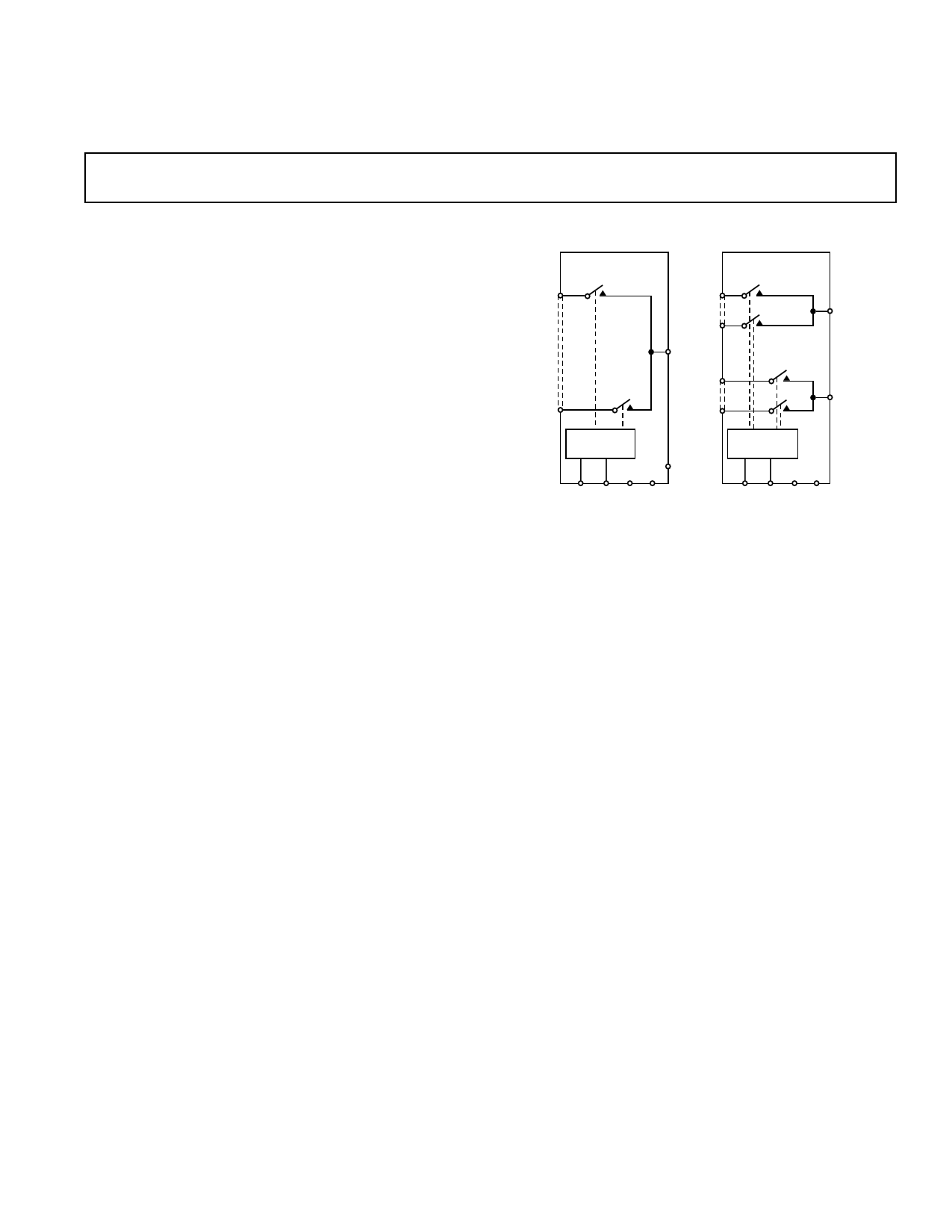
FUNCTIONAL BLOCK DIAGRAMS
ADG728
ADG729
S1 S1A
DA
S4A
D
S1B
DB
S8 S4B
INPUT SHIFT
REGISTER
RESET
SDA SCL A0 A1
INPUT SHIFT
REGISTER
SDA SCL A0 A1
GENERAL DESCRIPTION
The ADG728 and ADG729 are CMOS analog matrix switches
with a serially controlled 2-wire interface. The ADG728 is an
8-channel matrix switch, while the ADG729 is a dual 4-channel
matrix switch. On resistance is closely matched between switches
and very flat over the full signal range. These parts can operate
equally well as either multiplexers, demultiplexers or switch
arrays and the input signal range extends to the supplies.
The ADG728 and ADG729 utilize a 2-wire serial interface that
is compatible with the I2C™ interface standard. Both have two
external address pins (A0 and A1). This allows the 2 LSBs of
the 7-bit slave address to be set by the user. Four of each of the
devices can be connected to the one bus. The ADG728 also has
a RESET pin that should be tied high if not in use.
Each channel is controlled by one bit of an 8-bit word. This
means that these devices may be used in a number of different
configurations; all, any, or none of the channels may be on at
any one time.
On power-up of the device, all switches will be in the OFF con-
dition and the internal shift register will contain all zeros.
All channels exhibit break-before-make switching action pre-
venting momentary shorting when switching channels.
The ADG728 and ADG729 are available in 16-lead TSSOP
packages.
PRODUCT HIGHLIGHTS
1. 2-Wire Serial Interface.
2. Single Supply Operation. The ADG728 and ADG729 are
fully specified and guaranteed with 3 V and 5 V supply rails.
3. Low On Resistance 2.5 Ω typical.
4. Any configuration of switches may be on at any one time.
5. Guaranteed Break-Before-Make Switching Action.
6. Small 16-Lead TSSOP Package.
I2C is a trademark of Philips Corporation.
REV. 0
Information furnished by Analog Devices is believed to be accurate and
reliable. However, no responsibility is assumed by Analog Devices for its
use, nor for any infringements of patents or other rights of third parties
which may result from its use. No license is granted by implication or
otherwise under any patent or patent rights of Analog Devices.
One Technology Way, P.O. Box 9106, Norwood, MA 02062-9106, U.S.A.
Tel: 781/329-4700 World Wide Web Site: http://www.analog.com
Fax: 781/326-8703
© Analog Devices, Inc., 2000
1 page 
ADG728/ADG729
PIN FUNCTION DESCRIPTIONS
ADG728
1
2
3
4, 5, 6, 7
8
9, 10, 11, 12
13
14
15
16
ADG729
1
Mnemonic
SCL
RESET
3 SDA
4, 5, 6, 7
8, 9
10, 11, 12, 13
14
15
2
16
Sxx
Dx
Sxx
VDD
GND
A1
A0
Function
Serial Clock Line. This is used in conjunction with the SDA line to clock data into
the 8-bit input shift register. Clock rates of up to 400 kbit/s can be accommodated
with this 2-wire serial interface.
Active low control input that clears the input register and turns all switches to the
OFF condition.
Serial Data Line. This is used in conjunction with the SCL line to clock data into
the 8-bit input shift register during the write cycle and used to read back 1 byte of
data during the read cycle. It is a bidirectional open-drain data line which should be
pulled to the supply with an external pull-up resistor.
Source. May be an input or output.
Drain. May be an input or output.
Source. May be an input or output.
Power Supply Input. These parts can be operated from a supply of 2.7 V to 5.5 V.
Ground Reference.
Address Input. Sets the second least significant bit of the 7-bit slave address.
Address Input. Sets the least significant bit of the 7-bit slave address.
PIN CONFIGURATIONS
ADG728
ADG729
SCL 1
RESET 2
SDA 3
S1 4
S2 5
S3 6
S4 7
D8
ADG728
TOP VIEW
(Not to Scale)
16 A0
15 A1
14 GND
13 VDD
12 S5
11 S6
10 S7
9 S8
SCL 1
A1 2
SDA 3
S1A 4
S2A 5
S3A 6
S4A 7
DA 8
ADG729
TOP VIEW
(Not to Scale)
16 A0
15 GND
14 VDD
13 S1B
12 S2B
11 S3B
10 S4B
9 DB
Model
ADG728BRU
ADG729BRU
Temperature Range
–40°C to +85°C
–40°C to +85°C
ORDERING GUIDE
Package Description
Thin Shrink Small Outline Package (TSSOP)
Thin Shrink Small Outline Package (TSSOP)
Package Option
RU-16
RU-16
REV. 0
–5–
5 Page 
MULTIPLE DEVICES ON ONE BUS
Figure 20 shows four ADG728s devices on the same serial bus.
Each has a different slave address since the state of their A0 and
A1 pins is different. This allows each Matrix Switch to be writ-
ten to or read from independently. Because the ADG729 has a
different address to the ADG728, it would be possible for four
of each of these devices to be connected to the same bus.
MASTER
+5V
RP RP
ADG728/ADG729
SDA
SCL
SDA
SCL
A1
A0
ADG728
VDD
SDA
A1
SCL
A0
ADG728
VDD
SDA
A1
SCL
A0
ADG728
VDD
SDA
A1
SCL
A0
ADG728
Figure 20. Multiple ADG728s on the Same Bus
TEST CIRCUITS
IDS
V1
SD
VS
RON = V1/IDS
Test Circuit 1. On Resistance
IS (OFF)
A
VS
VD
S1
S2
S8
VDD
VDD
GND
D
S1
S2
S8
VS
VDD
VDD
GND
ID (OFF)
DA
VD
Test Circuit 3. IS (OFF)
VDD
VDD
S1
S8
ID (ON)
DA
VD
VS GND
Test Circuit 2. ID (OFF)
Test Circuit 4. ID (ON)
VDD
VDD
ADG728*
S1
S2 THRU S7
S8
GND
D
VS1
VS8
RL
300⍀
SCL
VOUT
CL
35pF
VS1
VOUT
50%
50%
90%
90%
VS1 = VS8
VOUT
* SIMILAR CONNECTION FOR ADG729
tOFF
tON
Test Circuit 5. Switching Times and Break-Before-Make Times
80%
80%
tOPEN
REV. 0
–11–
11 Page | ||
| Páginas | Total 12 Páginas | |
| PDF Descargar | [ Datasheet ADG729.PDF ] | |
Hoja de datos destacado
| Número de pieza | Descripción | Fabricantes |
| ADG721 | CMOS Low Voltage 4 ohm Dual SPST Switches | Analog Devices |
| ADG722 | CMOS Low Voltage 4 ohm Dual SPST Switches | Analog Devices |
| ADG723 | CMOS Low Voltage 4 ohm Dual SPST Switches | Analog Devices |
| ADG725 | 16-/32- Channel/ Serially Controlled 4 1.8 V to 5.5 V/ 2.5 V/ Analog Multiplexers | Analog Devices |
| Número de pieza | Descripción | Fabricantes |
| SLA6805M | High Voltage 3 phase Motor Driver IC. |
Sanken |
| SDC1742 | 12- and 14-Bit Hybrid Synchro / Resolver-to-Digital Converters. |
Analog Devices |
|
DataSheet.es es una pagina web que funciona como un repositorio de manuales o hoja de datos de muchos de los productos más populares, |
| DataSheet.es | 2020 | Privacy Policy | Contacto | Buscar |