|
|
|
PDF ADG528F Data sheet ( Hoja de datos )
| Número de pieza | ADG528F | |
| Descripción | 4/8 Channel Fault-Protected Analog Multiplexers | |
| Fabricantes | Analog Devices | |
| Logotipo | ||
Hay una vista previa y un enlace de descarga de ADG528F (archivo pdf) en la parte inferior de esta página. Total 12 Páginas | ||
|
No Preview Available !
a
4/8 Channel Fault-Protected
Analog Multiplexers
ADG508F/ADG509F/ADG528F*
FEATURES
Low On Resistance (300 ⍀ typ)
Fast Switching Times
tON 250 ns max
tOFF 250 ns max
Low Power Dissipation (3.3 mW max)
Fault and Overvoltage Protection (–40 V to +55 V)
All Switches OFF with Power Supply OFF
Analog Output of ON Channel Clamped Within Power
Supplies If an Overvoltage Occurs
Latch-Up Proof Construction
Break Before Make Construction
TTL and CMOS Compatible Inputs
APPLICATIONS
Existing Multiplexer Applications (Both Fault-Protected
and Nonfault-Protected)
New Designs Requiring Multiplexer Functions
GENERAL DESCRIPTION
The ADG508F, ADG509F and ADG528F are CMOS analog
multiplexers, the ADG508F and ADG528F comprising eight
single channels and the ADG509F comprising four differential
channels. These multiplexers provide fault protection. Using a
series n-channel, p-channel, n-channel MOSFET structure,
both device and signal source protection is provided in the event
of an overvoltage or power loss. The multiplexer can withstand
continuous overvoltage inputs from –40 V to +55 V. During
fault conditions, the multiplexer input (or output) appears as an
open circuit and only a few nanoamperes of leakage current will
flow. This protects not only the multiplexer and the circuitry
driven by the multiplexer, but also protects the sensors or signal
sources that drive the multiplexer.
The ADG508F and ADG528F switch one of eight inputs to a
common output as determined by the 3-bit binary address lines
A0, A1 and A2. The ADG509F switches one of four differential
inputs to a common differential output as determined by the 2-
bit binary address lines A0 and A1. The ADG528F has on-chip
address and control latches that facilitate microprocessor inter-
facing. An EN input on each device is used to enable or disable
the device. When disabled, all channels are switched OFF.
PRODUCT HIGHLIGHTS
1. Fault Protection.
The ADG508F/ADG509F/ADG528F can withstand con-
tinuous voltage inputs from –40 V to +55 V. When a fault
occurs due to the power supplies being turned off, all the
channels are turned off and only a leakage current of a few
nanoamperes flows.
*Patent Pending.
REV. C
Information furnished by Analog Devices is believed to be accurate and
reliable. However, no responsibility is assumed by Analog Devices for its
use, nor for any infringements of patents or other rights of third parties
which may result from its use. No license is granted by implication or
otherwise under any patent or patent rights of Analog Devices.
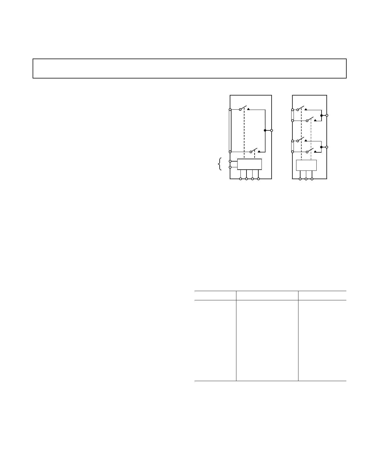
FUNCTIONAL BLOCK DIAGRAMS
ADG508F/ADG528F
S1
ADG509F
S1A
S4A
D
S1B
S8
ADG528F WR
ONLY RS
1 OF 8
DECODER
S4B
1 OF 4
DECODER
DA
DB
A0 A1 A2 EN
A0 A1 EN
2. ON channel turns off while fault exists.
3. Low RON.
4. Fast Switching Times.
5. Break-Before-Make Switching.
Switches are guaranteed break-before-make so that input
signals are protected against momentary shorting.
6. Trench Isolation Eliminates Latch-up.
A dielectric trench separates the p and n-channel MOSFETs
thereby preventing latch-up.
ORDERING GUIDE
Model1
Temperature Range Package Option2
ADG508FBN
ADG508FBRN
ADG508FBRW
ADG508FTQ
ADG509FBN
ADG509FBRN
ADG509FBRW
ADG509FTQ
ADG528FBN
ADG528FBP
ADG528FTQ
–40°C to +85°C
–40°C to +85°C
–40°C to +85°C
–55°C to +125°C
–40°C to +85°C
–40°C to +85°C
–40°C to +85°C
–55°C to +125°C
–40°C to +85°C
–40°C to +85°C
–55°C to +125°C
N-16
R-16N
R-16W
Q-16
N-16
R-16N
R-16W
Q-16
N-18
P-20A
Q-18
NOTES
1To order MIL-STD-883, Class B processed parts, add /883B to T grade part
numbers.
2N = Plastic DIP; P = Plastic Leaded Chip Carrier (PLCC); Q = Cerdip;
RN = 0.15" Small Outline IC (SOIC), RW = 0.3" Small Outline IC (SOIC).
One Technology Way, P.O. Box 9106, Norwood, MA 02062-9106, U.S.A.
Tel: 781/329-4700
World Wide Web Site: http://www.analog.com
Fax: 781/326-8703
© Analog Devices, Inc., 1998
1 page 
ADG508F/ADG509F/ADG528F
TERMINOLOGY
VDD
VSS
GND
RON
RON Drift
RON Match
IS (OFF)
ID (OFF)
ID, IS (ON)
VD (VS)
CS (OFF)
CD (OFF)
CD, CS (ON)
CIN
tON (EN)
tOFF (EN)
tTRANSITION
tOPEN
VINL
VINH
IINL (IINH)
Off Isolation
Charge Injection
IDD
ISS
Most positive power supply potential.
Most negative power supply potential.
Ground (0 V) reference.
Ohmic resistance between D and S.
Change in RON when temperature changes
by one degree Celsius.
Difference between the RON of any two
channels.
Source leakage current when the switch is
off.
Drain leakage current when the switch is off.
Channel leakage current when the switch is
on.
Analog voltage on terminals D, S.
Channel input capacitance for “OFF”
condition.
Channel output capacitance for “OFF”
condition.
“ON” switch capacitance.
Digital input capacitance.
Delay time between the 50% and 90% points
of the digital input and switch “ON”
condition.
Delay time between the 50% and 90% points
of the digital input and switch “OFF”
condition.
Delay time between the 50% and 90% points
of the digital inputs and the switch “ON”
condition when switching from one address
state to another.
“OFF” time measured between 80% points of
both switches when switching from one
address state to another.
Maximum input voltage for Logic “0”.
Minimum input voltage for Logic “1”.
Input current of the digital input.
A measure of unwanted signal coupling
through an “OFF” channel.
A measure of the glitch impulse transferred
from the digital input to the analog output
during switching.
Positive supply current.
Negative supply current.
Typical Performance Graphs
2000
1750
TA = +25؇C
1500
1250
1000
VDD = +5V
VSS = –5V
750
500
250
0
–15
–10
VDD = +10V
VSS = –10V
–5 0
5
VD (VS) – Volts
VDD = +15V
VSS = –15V
10
15
Figure 3. On Resistance as a Function of VD (VS)
1m
100
10
1
VDD = 0V
VSS = 0V
VD = 0V
100n
10n
OPERATING RANGE
1n
100p
10p
1p
–50 –40 –30 –20 –10 0 10 20 30 40 50 60
VIN – INPUT VOLTAGE – Volts
Figure 4. Input Leakage Current as a Function of VS
(Power Supplies OFF) During Overvoltage Conditions
1m
100
10
1
VDD = +15V
VSS = –15V
VD = 0V
100n
10n
OPERATING RANGE
1n
100p
10p
1p
–50 –40 –30 –20 –10 0 10 20 30 40 50 60
VIN – INPUT VOLTAGE – Volts
Figure 5. Output Leakage Current as a Function of VS
(Power Supplies ON) During Overvoltage Conditions
REV. C
–5–
5 Page 
ADG508F/ADG509F/ADG528F
16-Lead Plastic (N-16)
OUTLINE DIMENSIONS
Dimensions shown in inches and (mm).
16-Lead Cerdip (Q-16)
0.840 (21.34)
0.745 (18.92)
16
1
9 0.280 (7.11)
8 0.240 (6.10)
PIN 1
0.210 (5.33)
MAX
0.160 (4.06)
0.115 (2.93)
0.022 (0.558)
0.014 (0.356)
0.100
(2.54)
BSC
0.060 (1.52)
0.015 (0.38)
0.130
(3.30)
MIN
0.070 (1.77) SEATING
0.045 (1.15) PLANE
0.325 (8.26)
0.300 (7.62) 0.195 (4.95)
0.115 (2.93)
0.015 (0.381)
0.008 (0.204)
0.005 (0.13) MIN
0.080 (2.03) MAX
16 9
0.310 (7.87)
0.220 (5.59)
18
PIN 1
0.840 (21.34) MAX
0.060 (1.52)
0.200 (5.08)
MAX
0.200 (5.08)
0.125 (3.18)
0.023 (0.58)
0.014 (0.36)
0.100
(2.54)
BSC
0.015 (0.38)
0.150
(3.81)
MIN
0.070
(1.78)
SEATING
PLANE
0.030 (0.76)
0.320 (8.13)
0.290 (7.37)
0.015 (0.38)
15° 0.008 (0.20)
0°
16-Lead SOIC (R-16N)
(Narrow Body)
0.3937 (10.00)
0.3859 (9.80)
0.1574 (4.00) 16
0.1497 (3.80) 1
9
0.2440 (6.20)
8 0.2284 (5.80)
0.0098 (0.25)
0.0040 (0.10)
PIN 1
0.0688 (1.75)
0.0532 (1.35)
0.0196 (0.50)
0.0099 (0.25) x 45°
SEATING
0.0500
(1.27)
PLANE BSC
0.0192 (0.49)
0.0138 (0.35)
8°
0.0099 (0.25) 0° 0.0500 (1.27)
0.0075 (0.19) 0.0160 (0.41)
16-Lead SOIC (R-16W)
(Wide Body)
0.4133 (10.50)
0.3977 (10.00)
16 9
18
0.0118 (0.30)
0.0040 (0.10)
PIN 1
0.1043 (2.65)
0.0926 (2.35)
0.0291
0.0098
(0.74)
(0.25)
x
45°
0.0500
(1.27)
BSC
0.0192 (0.49)
0.0138 (0.35)
8°
SEATING 0.0125 (0.32) 0°
PLANE 0.0091 (0.23)
0.0500 (1.27)
0.0157 (0.40)
REV. C
–11–
11 Page | ||
| Páginas | Total 12 Páginas | |
| PDF Descargar | [ Datasheet ADG528F.PDF ] | |
Hoja de datos destacado
| Número de pieza | Descripción | Fabricantes |
| ADG528A | CMOS Latched 4-/8-Channel Analog Multiplexers | Analog Devices |
| ADG528F | 4/8 Channel Fault-Protected Analog Multiplexers | Analog Devices |
| Número de pieza | Descripción | Fabricantes |
| SLA6805M | High Voltage 3 phase Motor Driver IC. |
Sanken |
| SDC1742 | 12- and 14-Bit Hybrid Synchro / Resolver-to-Digital Converters. |
Analog Devices |
|
DataSheet.es es una pagina web que funciona como un repositorio de manuales o hoja de datos de muchos de los productos más populares, |
| DataSheet.es | 2020 | Privacy Policy | Contacto | Buscar |