|
|
|
PDF ADG508F Data sheet ( Hoja de datos )
| Número de pieza | ADG508F | |
| Descripción | 4/8 Channel Fault-Protected Analog Multiplexers | |
| Fabricantes | Analog Devices | |
| Logotipo | ||
Hay una vista previa y un enlace de descarga de ADG508F (archivo pdf) en la parte inferior de esta página. Total 20 Páginas | ||
|
No Preview Available !
8-Channel/4-Channel
Fault-Protected Analog Multiplexers
ADG508F/ADG509F
FEATURES
All switches off with power supply off
Analog output of on channel clamped within power
supplies if an overvoltage occurs
Latch-up proof construction
Low on resistance (270 Ω typical)
Fast switching times
tON: 230 ns maximum
tOFF: 130 ns maximum
Low power dissipation (3.3 mW maximum)
Fault and overvoltage protection (−40 V to +55 V)
Break-before-make construction
TTL and CMOS compatible inputs
APPLICATIONS
Existing multiplexer applications (both fault-protected and
nonfault-protected)
New designs requiring multiplexer functions
GENERAL DESCRIPTION
The ADG508F and ADG509F are CMOS analog multi-
plexers, with the ADG508F comprising eight single channels
and the ADG509F comprising four differential channels. These
multiplexers provide fault protection. Using a series n-channel,
p-channel, n-channel MOSFET structure, both device and signal
source protection is provided in the event of an overvoltage or
power loss. The multiplexer can withstand continuous overvolt-
age inputs from −40 V to +55 V. During fault conditions with
power supplies off, the multiplexer input (or output) appears as
an open circuit and only a few nanoamperes of leakage current
will flow. This protects not only the multiplexer and the circuitry
driven by the multiplexer, but also protects the sensors or signal
sources that drive the multiplexer.
The ADG508F switches one of eight inputs to a common output
as determined by the 3-bit binary address lines A0, A1, and A2.
The ADG509F switches one of four differential inputs to a
common differential output as determined by the 2-bit binary
address lines A0 and A1. An EN input on each device is used
to enable or disable the device. When disabled, all channels are
switched off.
Rev. F
Information furnished by Analog Devices is believed to be accurate and reliable. However, no
responsibility is assumed by Analog Devices for its use, nor for any infringements of patents or other
rights of third parties that may result from its use. Specifications subject to change without notice. No
license is granted by implication or otherwise under any patent or patent rights of Analog Devices.
Trademarksandregisteredtrademarksarethepropertyoftheirrespectiveowners.
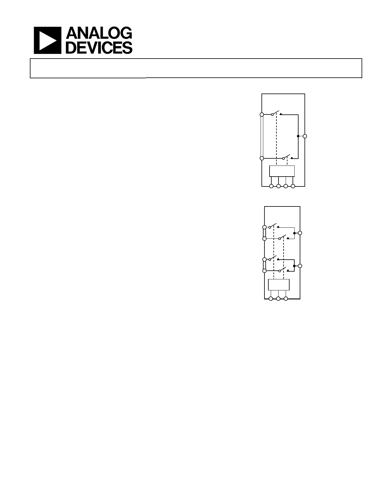
FUNCTIONAL BLOCK DIAGRAMS
ADG508F
S1
D
S8
1 OF 8
DECODER
A0 A1 A2 EN
Figure 1.
ADG509F
S1A
DA
S4A
S1B
S4B
1 OF 4
DECODER
DB
A0 A1 EN
Figure 2.
PRODUCT HIGHLIGHTS
1. Fault protection. The ADG508F/ADG509F can withstand
continuous voltage inputs from −40 V to +55 V. When a
fault occurs due to the power supplies being turned off, all
the channels are turned off and only a leakage current of a
few nanoamperes flows.
2. On channel saturates while fault exists.
3. Low RON.
4. Fast switching times.
5. Break-before-make switching. Switches are guaranteed
break-before-make so that input signals are protected
against momentary shorting.
6. Trench isolation eliminates latch-up. A dielectric trench
separates the p and n-channel MOSFETs thereby
preventing latch-up.
One Technology Way, P.O. Box 9106, Norwood, MA 02062-9106, U.S.A.
Tel: 781.329.4700
www.analog.com
Fax: 781.461.3113 ©2001–2011 Analog Devices, Inc. All rights reserved.
1 page 
ABSOLUTE MAXIMUM RATINGS
TA = 25°C unless otherwise noted.
Table 4.
Parameter
VDD to VSS
VDD to GND
VSS to GND
Digital Input, EN, Ax
VS, Analog Input Overvoltage with
Power On (VDD = +15 V, VSS = −15 V)
VS, Analog Input Overvoltage with
Power Off (VDD = 0 V, VSS = 0 V)
Continuous Current, S or D
Peak Current, S or D
(Pulsed at 1 ms, 10% Duty Cycle Max)
Operating Temperature Range
Industrial (B Version)
Storage Temperature Range
Junction Temperature
TSSOP
θJA, Thermal Impedance
Plastic DIP Package
θJA, Thermal Impedance
16-Lead
SOIC Package
θJA, Thermal Impedance
Narrow Body
Wide Body
Rating
48 V
−0.3 V to +48 V
+0.3 V to −48 V
−0.3 V to VDD + 0.3 V or
20 mA, whichever occurs first
VSS − 25 V to VDD + 40 V
−40 V to +55 V
20 mA
40 mA
−40°C to +85°C
−65°C to +150°C
150°C
112°C/W
117°C/W
77°C/W
75°C/W
ADG508F/ADG509F
Stresses above those listed under Absolute Maximum Ratings
may cause permanent damage to the device. This is a stress
rating only; functional operation of the device at these or any
other conditions above those indicated in the operational
section of this specification is not implied. Exposure to absolute
maximum rating conditions for extended periods may affect
device reliability.
ESD CAUTION
Rev. F | Page 5 of 20
5 Page 
THEORY OF OPERATION
The ADG508F/ADG509F multiplexers are capable of withstand-
ing overvoltages from −40 V to +55 V, irrespective of whether the
power supplies are present or not. Each channel of the multiplexer
consists of an n-channel MOSFET, a p-channel MOSFET, and an
n-channel MOSFET, connected in series. When the analog input
exceeds the power supplies, one of the MOSFETs will saturate
limiting the current. The current during a fault condition is
determined by the load on the output. Figure 17 illustrates
the channel architecture that enables these multiplexers to
withstand continuous overvoltages.
When an analog input of VSS + 2.2 V to VDD − 2.2 V (output
loaded, 1 mA) is applied to the ADG508F/ADG509F, the
multiplexer behaves as a standard multiplexer, with spec-
ifications similar to a standard multiplexer, for example,
the on-resistance is 390 Ω maximum. However, when an
overvoltage is applied to the device, one of the three
MOSFETs saturate.
Figure 17 to Figure 20 show the conditions of the three MOSFETs
for the various overvoltage situations. When the analog input
applied to an on channel approaches the positive power supply
line, the n-channel MOSFET saturates because the voltage on
the analog input exceeds the difference between VDD and the
n-channel threshold voltage (VTN). When a voltage more nega-
tive than VSS is applied to the multiplexer, the p-channel
MOSFET will saturate because the analog input is more
negative than the difference between VSS and the p-channel
threshold voltage (VTP). Because VTN is nominally 1.4 V and
VTP −1.4 V, the analog input range to the multiplexer is limited
to VSS + 1.4 V to VDD – 1.4 V (output open circuit) when a
±15 V power supply is used.
When the power supplies are present but the channel is off,
again either the p-channel MOSFET or one of the n-channel
MOSFETs will remain off when an overvoltage occurs.
Finally, when the power supplies are off, the gate of each
MOSFET will be at ground. A negative overvoltage switches
on the first n-channel MOSFET but the bias produced by the
overvoltage causes the p-channel MOSFET to remain turned
off. With a positive overvoltage, the first MOSFET in the series
will remain off because the gate to source voltage applied to this
MOSFET is negative.
ADG508F/ADG509F
During fault conditions (power supplies off), the leakage
current into and out of the ADG508F/ADG509F is limited to
a few microamps. This protects the multiplexer and succeeding
circuitry from over stresses as well as protecting the signal
sources which drive the multiplexer. Also, the other channels
of the multiplexer will be undisturbed by the overvoltage and
will continue to operate normally.
+55V
OVERVOLTAGE
Q1 Q2 Q3
n-CHANNEL
MOSFET
SATURATES
VDD
VSS
Figure 17. +55 V Overvoltage Input to the On Channel
–40V
OVERVOLTAGE
Q1 Q2 Q3
n-CHANNEL
MOSFET
IS ON
VSS
p-CHANNEL
MOSFET
VDD SATURATES
Figure 18. −40 V Overvoltage on an Off Channel with
Multiplexer Power On
+55V
OVERVOLTAGE
Q1 Q2 Q3
n-CHANNEL
MOSFET IS
OFF
Figure 19. +55 V Overvoltage with Power Off
–40V
OVERVOLTAGE
Q1 Q2 Q3
n-CHANNEL
MOSFET IS
ON
p-CHANNEL
MOSFET IS
OFF
Figure 20. −40 V Overvoltage with Power Off
Rev. F | Page 11 of 20
11 Page | ||
| Páginas | Total 20 Páginas | |
| PDF Descargar | [ Datasheet ADG508F.PDF ] | |
Hoja de datos destacado
| Número de pieza | Descripción | Fabricantes |
| ADG508A | CMOS 4/8 CHAANNEL ANALOG MULTIPLEXERS | Analog Devices |
| ADG508F | 4/8 Channel Fault-Protected Analog Multiplexers | Analog Devices |
| Número de pieza | Descripción | Fabricantes |
| SLA6805M | High Voltage 3 phase Motor Driver IC. |
Sanken |
| SDC1742 | 12- and 14-Bit Hybrid Synchro / Resolver-to-Digital Converters. |
Analog Devices |
|
DataSheet.es es una pagina web que funciona como un repositorio de manuales o hoja de datos de muchos de los productos más populares, |
| DataSheet.es | 2020 | Privacy Policy | Contacto | Buscar |