|
|
|
PDF ADG426 Data sheet ( Hoja de datos )
| Número de pieza | ADG426 | |
| Descripción | LC2MOS 8-/16-Channel High Performance Analog Multiplexers | |
| Fabricantes | Analog Devices | |
| Logotipo | ||
Hay una vista previa y un enlace de descarga de ADG426 (archivo pdf) en la parte inferior de esta página. Total 12 Páginas | ||
|
No Preview Available !
a
LC2MOS 8-/16-Channel
High Performance Analog Multiplexers
ADG406/ADG407/ADG426
FEATURES
44 V Supply Maximum Ratings
VSS to VDD Analog Signal Range
Low On Resistance (80 Ω max)
Low Power
Fast Switching
tON < 160 ns
tOFF < 150 ns
Break Before Make Switching Action
Plug-In Upgrade for
DG506A/ADG506A, DG507A/ADG507A,
DG526/ADG526A
ADG406/ADG407 are Plug-In Replacements for
DG406/DG407
APPLICATIONS
Audio and Video Routing
Automatic Test Equipment
Data Acquisition Systems
Battery Powered Systems
Sample Hold Systems
Communication Systems
Avionics
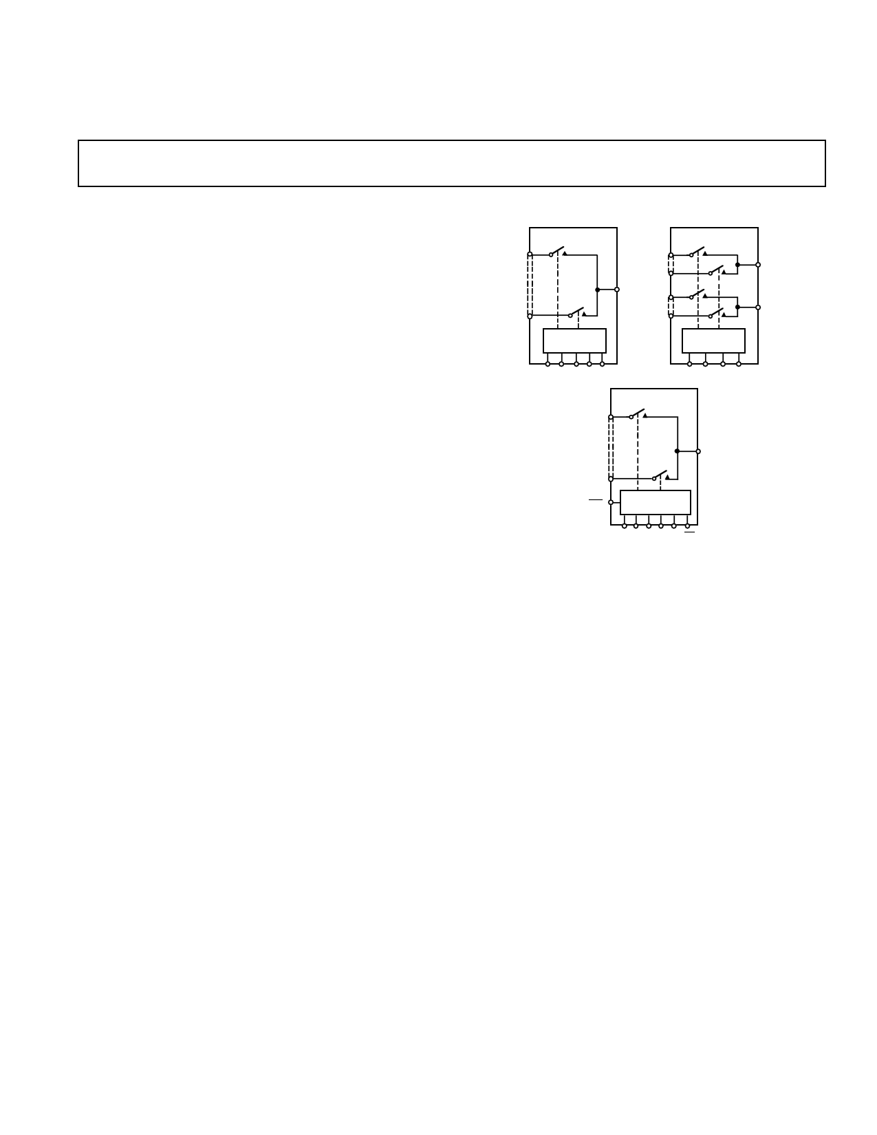
FUNCTIONAL BLOCK DIAGRAMS
ADG406
ADG407
S1 S1A
DA
S8A
D
S1B
DB
S16 S8B
1 OF 16
DECODER
1 OF 8
DECODER
A0 A1 A2 A3 EN
S1
A0 A1 A2 EN
ADG426
D
S16
DECODER/
WR LATCHES
A0 A1 A2 A3 EN RS
GENERAL DESCRIPTION
The ADG406, ADG407 and ADG426 are monolithic CMOS
analog multiplexers. The ADG406 and ADG426 switch one of
sixteen inputs to a common output as determined by the 4-bit
binary address lines A0, A1, A2 and A3. The ADG426 has on-
chip address and control latches that facilitate microprocessor
interfacing. The ADG407 switches one of eight differential
inputs to a common differential output as determined by the 3-
bit binary address lines A0, A1 and A2. An EN input on all
devices is used to enable or disable the device. When disabled,
all channels are switched OFF.
The ADG406/ADG407/ADG426 are designed on an enhanced
LC2MOS process that provides low power dissipation yet gives
high switching speed and low on resistance. These features
make the parts suitable for high speed data acquisition systems
and audio signal switching. Low power dissipation makes the
parts suitable for battery powered systems. Each channel
conducts equally well in both directions when ON and has an
input signal range which extends to the supplies. In the OFF
condition, signal levels up to the supplies are blocked. All
channels exhibit break before make switching action preventing
momentary shorting when switching channels. Inherent in the
design is low charge injection for minimum transients when
switching the digital inputs.
PRODUCT HIGHLIGHTS
1. Extended Signal Range
The ADG406/ADG407/ADG426 are fabricated on an
enhanced LC2MOS process giving an increased signal range
which extends to the supply rails
2. Low Power Dissipation
3. Low R
ON
4. Single/Dual Supply Operation
5. Single Supply Operation
For applications where the analog signal is unipolar, the
ADG406/ADG407/ADG426 can be operated from a single
rail power supply. The parts are fully specified with a single
+12 V power supply and will remain functional with single
supplies as low as +5 V.
REV. 0
Information furnished by Analog Devices is believed to be accurate and
reliable. However, no responsibility is assumed by Analog Devices for its
use, nor for any infringements of patents or other rights of third parties
which may result from its use. No license is granted by implication or
otherwise under any patent or patent rights of Analog Devices.
One Technology Way, P.O. Box 9106, Norwood. MA 02062-9106, U.S.A.
Tel: 617/329-4700
Fax: 617/326-8703
1 page 
Table I. Truth Table (ADG406)
A3 A2 A1 A0 EN ON SWITCH
XXXX0
00001
00011
00101
00111
01001
01011
01101
01111
10001
10011
10101
10111
11001
11011
11101
11111
NONE
1
2
3
4
5
6
7
8
9
10
11
12
13
14
15
16
Table II. Truth Table (ADG407)
A2 A1 A0 EN ON SWITCH PAIR
XXX0
0001
0011
0101
0111
1001
1011
1101
1111
NONE
1
2
3
4
5
6
7
8
Table III. Truth Table (ADG426)
A3 A2 A1 A0 EN WR RS ON SWITCH
XXXXX
1
XXXXXX0
XXXX0 0 1
0000101
0001101
0010101
0011101
0100101
0101101
0110101
0111101
1000101
1001101
1010101
1011101
1100101
1101101
1110101
1111101
Retains Previous
Switch Condition
NONE (Address
and Enable
Latches Cleared)
NONE
1
2
3
4
5
6
7
8
9
10
11
12
13
14
15
16
ADG406/ADG407/ADG426
PIN CONFIGURATIONS
DIP PLCC
VDD 1
NC 2
NC 3
28 D
27 VSS
26 S8
S16 4
25 S7
S15 5
24 S6
S14 6
23 S5
S13 7 ADG406 22 S4
TOP VIEW
S12 8 (Not to Scale) 21 S3
S11 9
20 S2
S10 10
19 S1
S9 11
18 EN
GND 12
17 A0
NC 13
16 A1
A3 14
15 A2
4 3 2 1 28 27 26
S15 5
S14 6
S13 7
S12 8
S11 9
S10 10
S9 11
ADG406
TOP VIEW
(Not to Scale)
25 S7
24 S6
23 S5
22 S4
21 S3
20 S2
19 S1
12 13 14 15 16 17 18
NC = NO CONNECT
VDD 1
DB 2
NC 3
28 DA
27 VSS
26 S8A
S8B 4
25 S7A
S7B 5
24 S6A
S6B 6
23 S5A
S5B 7 ADG407 22 S4A
TOP VIEW
S4B 8 (Not to Scale) 21 S3A
S3B 9
20 S2A
S2B 10
19 S1A
S1B 11
18 EN
GND 12
17 A0
NC 13
16 A1
NC 14
15 A2
4 3 2 1 28 27 26
S7B 5
S6B 6
S5B 7
S4B 8
S3B 9
S2B 10
S1B 11
ADG407
TOP VIEW
(Not to Scale)
25 S7A
24 S6A
23 S5A
22 S4A
21 S3A
20 S2A
19 S1A
12 13 14 15 16 17 18
NC = NO CONNECT
PIN CONFIGURATION
DIP/SSOP
VDD 1
28 D
NC 2
27 VSS
RS 3
26 S8
S16 4
25 S7
S15 5
24 S6
S14 6
23 S5
S13 7 ADG426 22 S4
TOP VIEW
S12 8 (Not to Scale) 21 S3
S11 9
20 S2
S10 10
19 S1
S9 11
18 EN
GND 12
17 A0
WR 13
16 A1
A3 14
15 A2
NC = NO CONNECT
REV. 0
–5–
5 Page 
VDD
VSS
2.4V
VRS
VDD
A3
VSS
S1
A2 S2 THRU S16
A1
ADG426
A0
EN D
RS
WR GND
VWR
VS
RL
300Ω
VOUT
CL
35pF
3V
WR
0V
V0
OUTPUT
0V
ADG406/ADG407/ADG426
50%
tON(WR)
0.2V0
Test Circuit 8.
Write
Turn-On
Time,
t
ON
(WR)
2.4V
VIN
VDD
VSS
VDD
A3
VSS
S1
A2 S2 THRU S16
A1 ADG426
A0
EN
RS D
GND WR
3V
VS
RS
0V
RL
300Ω
VOUT
CL
35pF
V0
OUTPUT
0V
50%
tOFF (RS)
0.8V0
Test Circuit 9. Reset Turn-Off Time, tOFF (RS)
VS RS
VIN
VDD
VSS
VDD
A3
A2
VSS
RS
A1
ADG426*
A0
SD
EN
GND WR
2.4V
VOUT
CL
1nF
3V
LOGIC
INPUT
(VIN)
VOUT
QINJ = CL x ∆VOUT
∆ VOUT
*SIMILAR CONNECTION FOR ADG406/ADG407
Test Circuit 10. Charge Injection
REV. 0
–11–
11 Page | ||
| Páginas | Total 12 Páginas | |
| PDF Descargar | [ Datasheet ADG426.PDF ] | |
Hoja de datos destacado
| Número de pieza | Descripción | Fabricantes |
| ADG426 | LC2MOS 8-/16-Channel High Performance Analog Multiplexers | Analog Devices |
| ADG428 | LC2MOS Latchable 4-/8-Channel High Performance Analog Multiplexers | Analog Devices |
| ADG429 | LC2MOS Latchable 4-/8-Channel High Performance Analog Multiplexers | Analog Devices |
| Número de pieza | Descripción | Fabricantes |
| SLA6805M | High Voltage 3 phase Motor Driver IC. |
Sanken |
| SDC1742 | 12- and 14-Bit Hybrid Synchro / Resolver-to-Digital Converters. |
Analog Devices |
|
DataSheet.es es una pagina web que funciona como un repositorio de manuales o hoja de datos de muchos de los productos más populares, |
| DataSheet.es | 2020 | Privacy Policy | Contacto | Buscar |