|
|
|
PDF ADF4211 Data sheet ( Hoja de datos )
| Número de pieza | ADF4211 | |
| Descripción | Dual RF/IF PLL Frequency Synthesizers | |
| Fabricantes | Analog Devices | |
| Logotipo | ||
Hay una vista previa y un enlace de descarga de ADF4211 (archivo pdf) en la parte inferior de esta página. Total 20 Páginas | ||
|
No Preview Available !
a Dual RF/IF PLL Frequency Synthesizers
ADF4210/ADF4211/ADF4212/ADF4213
FEATURES
ADF4210: 550 MHz/1.2 GHz
ADF4211: 550 MHz/2.0 GHz
ADF4212: 1.0 GHz/2.7 GHz
ADF4213: 1.0 GHz/3 GHz
2.7 V to 5.5 V Power Supply
Separate Charge Pump Supply (VP) Allows Extended
Tuning Voltage in 3 V Systems
Programmable Dual Modulus Prescaler
RF and IF: 8/9, 16/17, 32/33, 64/65
Programmable Charge Pump Currents
3-Wire Serial Interface
Analog and Digital Lock Detect
Fastlock Mode
Power-Down Mode
GENERAL DESCRIPTION
The ADF4210/ADF4211/ADF4212/ADF4213 is a dual frequency
synthesizer that can be used to implement local oscillators (LO)
in the upconversion and downconversion sections of wireless
receivers and transmitters. They can provide the LO for both
the RF and IF sections. They consist of a low-noise digital PFD
(Phase Frequency Detector), a precision charge pump, a pro-
grammable reference divider, programmable A and B Counters
and a dual-modulus prescaler (P/P + 1). The A (6-bit) and B
(12-bit) counters, in conjunction with the dual modulus prescaler
(P/P + 1), implement an N divider (N = BP + A). In addition,
the 14-bit reference counter (R Counter), allows selectable
REFIN frequencies at the PFD input. A complete PLL (Phase-
Locked Loop) can be implemented if the synthesizer is used with
an external loop filter and VCO (Voltage Controlled Oscillators).
APPLICATIONS
Base Stations for Wireless Radio (GSM, PCS, DCS,
CDMA, WCDMA)
Wireless Handsets (GSM, PCS, DCS, CDMA, WCDMA)
Control of all the on-chip registers is via a simple 3-wire interface.
The devices operate with a power supply ranging from 2.7 V to
5 V and can be powered down when not in use.
Wireless LANS
Communications Test Equipment
CATV Equipment
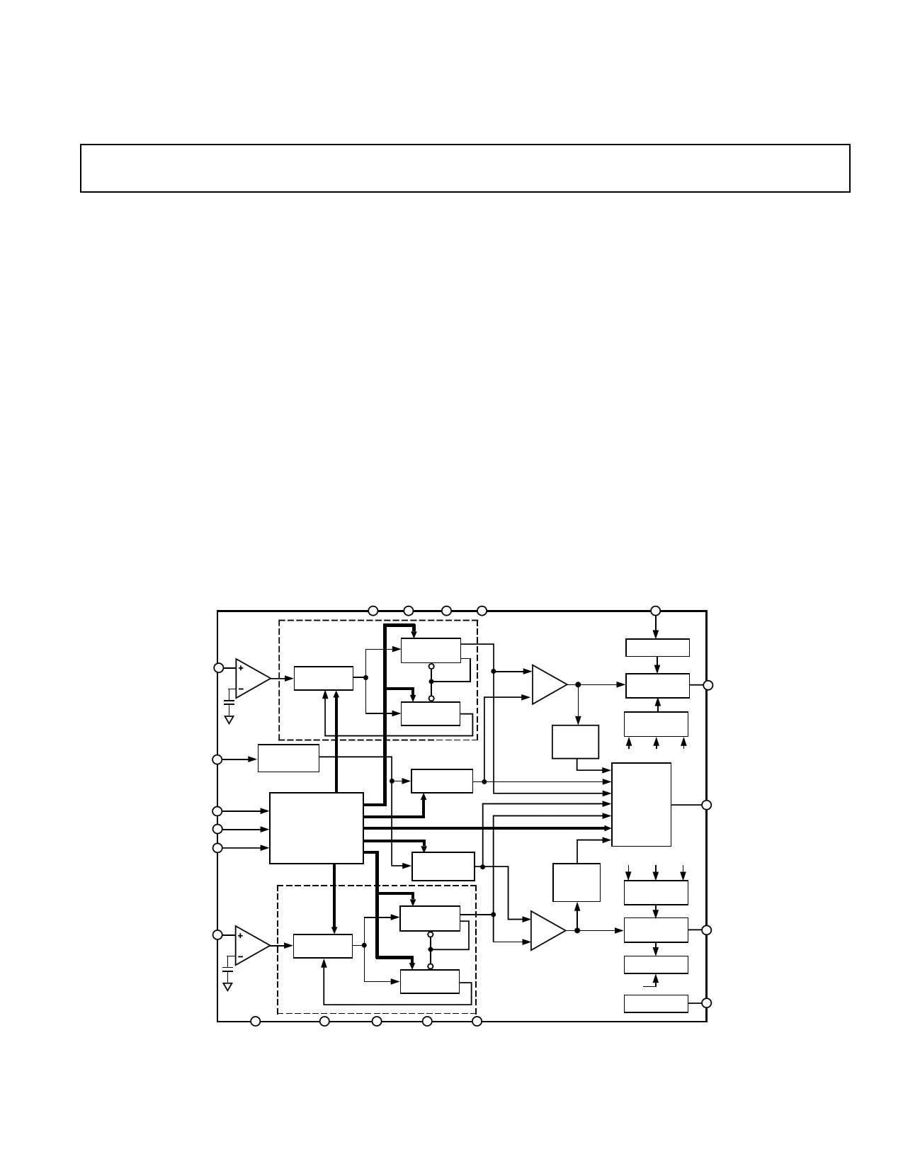
FUNCTIONAL BLOCK DIAGRAM
VDD1 VDD2 VP1 VP2
RSET
IFIN
REFIN
CLOCK
DATA
LE
RFIN
IF
PRESCALER
OSCILLATOR
24-BIT
DATA SDOUT
REGISTER
RF
PRESCALER
12-BIT IF
B-COUNTER
8-BIT IF
A-COUNTER
14-BIT IF
R-COUNTER
PHASE
COMPARATOR
REFERENCE
CHARGE
PUMP
CPIF
IF
LOCK
DETECT
IF CURRENT
SETTING
IFCP3 IFCP2 IFCP1
OUTPUT
MUX
MUXOUT
14-BIT RF
R-COUNTER
12-BIT RF
B-COUNTER
6-BIT RF
A-COUNTER
RF
LOCK
DETECT
RFCP3 RFCP2 RFCP1
IF CURRENT
SETTING
PHASE
COMPARATOR
CHARGE
PUMP
REFERENCE
ADF4210/ADF4211/
ADF4212/ADF4213
RSET
FLO SWITCH
CPRF
FLO
REV. A
DGNDRF
AGNDRF DGNDIF DGNDIF
Information furnished by Analog Devices is believed to be accurate and
reliable. However, no responsibility is assumed by Analog Devices for its
use, nor for any infringements of patents or other rights of third parties that
may result from its use. No license is granted by implication or otherwise
under any patent or patent rights of Analog Devices.
AGNDIF
One Technology Way, P.O. Box 9106, Norwood, MA 02062-9106, U.S.A.
Tel: 781/329-4700
www.analog.com
Fax: 781/326-8703
© Analog Devices, Inc., 2001
1 page 
Pin Number
TSSOP
1
Mnemonic
VDD1
2 VP1
3 CPRF
4 DGNDRF
5 RFIN
6 AGNDRF
7 FLO
8 REFIN
9 DGNDIF
10 MUXOUT
11 CLK
12 DATA
13 LE
14 RSET
15 AGNDIF
16 IFIN
17 DGNDIF
18 CPIF
19 VP2
20 VDD2
ADF4210/ADF4211/ADF4212/ADF4213
PIN FUNCTION DESCRIPTIONS
Function
Power Supply for the RF Section. Decoupling capacitors to the ground plane should be placed as
close as possible to this pin. VDD1 should have a value of between 2.7 V and 5.5 V. VDD1 must have
the same potential as VDD2.
Power Supply for the RF Charge Pump. This should be greater than or equal to VDD1. In systems where
VDD1 is 3 V, it can be set to 6 V and used to drive a VCO with a tuning range up to 6 V.
Output from the RF Charge Pump. This is normally connected to a loop filter which drives the input
to an external VCO.
Ground Pin for the RF Digital Circuitry.
Input to the RF Prescaler. This low level input signal is ac-coupled from the RF VCO.
Ground Pin for the RF Analog Circuitry.
RF/IF Fastlock Mode.
Reference Input. This is a CMOS input with a nominal threshold of VDD/2 and an equivalent input
resistance of 100 kΩ. This input can be driven from a TTL or CMOS crystal oscillator.
Digital Ground for the IF Digital, Interface and Control Circuitry.
This multiplexer output allows either the IF/RF Lock Detect, the scaled RF, scaled IF or the scaled
Reference Frequency to be accessed externally.
Serial Clock Input. This serial clock is used to clock in the serial data to the registers. The data is
latched into the 24-bit shift register on the CLK rising edge. This input is a high impedance
CMOS input.
Serial Data Input. The serial data is loaded MSB first with the two LSBs being the control bits. This
input is a high impedance CMOS input.
Load Enable, CMOS Input. When LE goes high, the data stored in the shift registers is loaded into
one of the four latches, the latch being selected using the control bits.
Connecting a resistor between this pin and ground sets the maximum RF and IF charge pump output
current. The nominal voltage potential at the RSET pin is 0.66 V. The relationship between ICP and RSET is
ICP MAX
=
13.5
RSET
So, with RSET = 2.7 kΩ, ICP MAX = 5 mA for both the RF and IF Charge Pumps.
Ground Pin for the IF Analog Circuitry.
Input to the RF Prescaler. This low-level input signal is ac-coupled from the IF VCO.
Ground Pin for the IF Digital, Interface, and Control Circuitry.
Output from the IF Charge Pump. This is normally connected to a loop filter which drives the input
to an external VCO.
Power Supply for the IF Charge Pump. This should be greater than or equal to VDD2. In systems where
VDD2 is 3 V, it can be set to 6 V and used to drive a VCO with a tuning range up to 6 V.
Power Supply for the IF, Digital and Interface Section. Decoupling capacitors to the ground plane should
be placed as close as possible to this pin. VDD2 should have a value of between 2.7 V and 5.5 V. VDD2
must have the same potential as VDD1.
TSSOP
PIN CONFIGURATIONS
CP-20
REV. A
VDD1 1
20 VDD2
VP1 2 ADF4210/ 19 VP2
CPRF 3 ADF4211/ 18 CPIF
DGNDRF 4 ADF4212/ 17 DGNDIF
RFIN 5 ADF4213 16 IFIN
AGNDRF 6 TOP VIEW 15 AGNDIF
(Not to Scale)
FLO 7
14 RSET
REFIN 8
13 LE
DGNDIF 9
12 DATA
MUXOUT 10
11 CLK
–5–
20 19 18 17 16
CPRF 1
DGNDRF 2
RFIN 3
AGNDRF 4
FLO 5
ADF4210/
ADF4211/
ADF4212/
ADF4213
TOP VIEW
(Not to Scale)
15 DGNDIF
14 IFIN
13 AGNDIF
12 RSET
11 LE
6 7 8 9 10
5 Page 
ADF4210/ADF4211/ADF4212/ADF4213
Table II. ADF421x Family Latch Summary
IF R COUNTER LATCH
IF CP CURRENT
SETTING
15-BIT REFERENCE COUNTER
CONTROL
BITS
DB23 DB22 DB21 DB20 DB19 DB18 DB17 DB16 DB15 DB14 DB13 DB12 DB11 DB10
IF IF IF
CP2 CP1 CP0
P4
P3
P2 P1 R15 R14 R13 R12 R11 R10 R9
DB9
R8
DB8
R7
DB7
R6
DB6 DB5 DB4 DB3 DB2 DB1 DB0
R5 R4 R3 R2 R1 C2 (0) C1 (0)
IF N COUNTER LATCH
IF
PRESCALER
12-BIT B COUNTER
6-BIT A COUNTER
CONTROL
BITS
DB23 DB22 DB21 DB20 DB19 DB18 DB17 DB16 DB15 DB14 DB13 DB12 DB11 DB10 DB9 DB8 DB7 DB6 DB5 DB4 DB3 DB2 DB1 DB0
P8 P7 P6 P5 B12 B11 B10 B9 B8 B7 B6 B5 B4 B3 B2 B1 A6 A5 A4 A3 A2 A1 C2 (0) C1 (1)
RF R COUNTER LATCH
RF CP CURRENT
SETTING
15-BIT REFERENCE COUNTER
CONTROL
BITS
DB23 DB22 DB21 DB20 DB19 DB18 DB17 DB16 DB15 DB14 DB13 DB12 DB11 DB10
RF
CP2
RF
CP1
RF
CP0
P12
P11
P10
P9
R15 R14
R13
R12
R11
R10
R9
DB9
R8
DB8
R7
DB7
R6
DB6 DB5 DB4 DB3 DB2 DB1 DB0
R5 R4 R3 R2 R1 C2 (1) C1 (0)
RF N COUNTER LATCH
RF
PRESCALER
12-BIT B COUNTER
6-BIT A COUNTER
CONTROL
BITS
DB23 DB22 DB21 DB20 DB19 DB18 DB17 DB16 DB15 DB14 DB13 DB12 DB11 DB10 DB9 DB8 DB7 DB6 DB5 DB4 DB3 DB2 DB1 DB0
P17 P16 P15 P14 B12 B11 B10 B9 B8 B7 B6 B5 B4 B3 B2 B1 A6 A5 A4 A3 A2 A1 C2 (1) C1 (1)
REV. A
–11–
11 Page | ||
| Páginas | Total 20 Páginas | |
| PDF Descargar | [ Datasheet ADF4211.PDF ] | |
Hoja de datos destacado
| Número de pieza | Descripción | Fabricantes |
| ADF4210 | Dual RF/IF PLL Frequency Synthesizers | Analog Devices |
| ADF4211 | Dual RF/IF PLL Frequency Synthesizers | Analog Devices |
| ADF4212 | Dual RF/IF PLL Frequency Synthesizers | Analog Devices |
| ADF4213 | Dual RF/IF PLL Frequency Synthesizers | Analog Devices |
| Número de pieza | Descripción | Fabricantes |
| SLA6805M | High Voltage 3 phase Motor Driver IC. |
Sanken |
| SDC1742 | 12- and 14-Bit Hybrid Synchro / Resolver-to-Digital Converters. |
Analog Devices |
|
DataSheet.es es una pagina web que funciona como un repositorio de manuales o hoja de datos de muchos de los productos más populares, |
| DataSheet.es | 2020 | Privacy Policy | Contacto | Buscar |