|
|
|
PDF ADC912AFP Data sheet ( Hoja de datos )
| Número de pieza | ADC912AFP | |
| Descripción | CMOS Microprocessor-Compatible 12-Bit A/D Converter | |
| Fabricantes | Analog Devices | |
| Logotipo | ||
Hay una vista previa y un enlace de descarga de ADC912AFP (archivo pdf) en la parte inferior de esta página. Total 16 Páginas | ||
|
No Preview Available !
a
CMOS Microprocessor-Compatible
12-Bit A/D Converter
FEATURES
Low Cost
Low Transition Noise between Code
12-Bit Accurate
؎1/2 LSB Nonlinearity Error over Temperature
No Missing Codes at All Temperatures
10 s Conversion Time
Internal or External Clock
8- or 16-Bit Data Bus Compatible
Improved ESD Resistant Design
Latchup Resistant Epi-CMOS Processing
Low 95 mW Power Consumption
Space-Saving 24-Lead 0.3" DIP, or 24-Lead SOIC
APPLICATIONS
Data Acquisition Systems
DSP System Front End
Process Control Systems
Portable Instrumentation
GENERAL DESCRIPTION
The ADC912A is a monolithic 12-bit accurate CMOS A/D
converter. It contains a complete successive-approximation A/D
converter built with a high-accuracy D/A converter, a precision
bipolar transistor high-speed comparator, and successive-
approximation logic including three-state bus interface for logic
compatibility. The accuracy of the ADC912A results from the
addition of precision bipolar transistors to Analog Devices’
advanced-oxide isolated silicon-gate CMOS process. Particular
attention was paid to the reduction of transition noise between
adjacent codes achieving a 1/6 LSB uncertainty. The low noise
design produces the same digital output for dc analog inputs
ADC912A
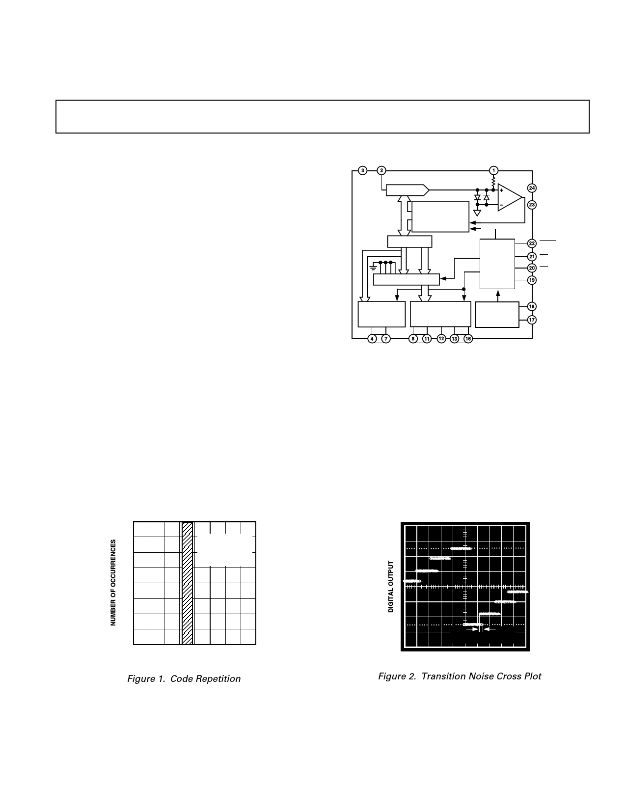
FUNCTIONAL BLOCK DIAGRAM
AGND VREFIN
AIN
12-BIT DAC
5k⍀
ADC912A
SUCCESSIVE
APPROXIMATION
REGISTER
12-BIT LATCH
48
MULTIPLEXER
8
THREE-STATE
OUTPUT
DRIVERS
THREE-STATE
OUTPUT
DRIVERS
CONTROL
LOGIC
CLOCK
OSCILLATOR
VDD
VSS
BUSY
CS
RD
HBEN
CLK OUT
CLK IN
D11 D8
D7 D4 DGND D3/11 D0/8
not located at a transition voltage, see Figures 1 and 2. NPN
digital output transistors provide excellent bus interface timing,
125 ns access and bus disconnect time which results in faster
data transfer without the need for wait states. An external
1.25 MHz clock provides a 10 µs conversion time.
In stand-alone applications an internal clock can be used with
external crystal.
An external negative five-volt reference sets the 0 V to 10 V
input range. Plus 5 V and minus 12 V power supplies result in
95 mW of total power consumption.
256
256 SUCCESSIVE
CONVERSIONS
192 WITH
AIN = 4.99756V
128
100
90
64
0
2045 2046 2047 2048 2049
OUTPUT CODE – Decimal
Figure 1. Code Repetition
10
0%
TRANSITION NOISE
ANALOG INPUT
Figure 2. Transition Noise Cross Plot
REV. B
Information furnished by Analog Devices is believed to be accurate and
reliable. However, no responsibility is assumed by Analog Devices for its
use, nor for any infringements of patents or other rights of third parties that
may result from its use. No license is granted by implication or otherwise
under any patent or patent rights of Analog Devices.
One Technology Way, P.O. Box 9106, Norwood, MA 02062-9106, U.S.A.
Tel: 781/329-4700
www.analog.com
Fax: 781/326-8703
© Analog Devices, Inc., 2001
1 page 
ADC912A
WAFER TEST LIMITS (@ VDD = +5 V, VSS = –12 V or –15 V, VREF = –5 V, AIN = 0 V to 10 V, and TA = 25؇C, unless otherwise noted.)
Parameter
Symbol Conditions
ADC912AG
Limit
Unit
Integral Nonlinearity
Differential Nonlinearity
Offset Error
Gain Error
Analog Input Resistance
Logic Input High Voltage
Logic Input Low Voltage
Logic Input Current
Logic Output High Voltage
Logic Output Low Voltage
Positive Supply Current
Negative Supply Current
INL
DNL
VZSE
GFSE
RAIN
VINH
VINL
IIN
VOH
VOL
IDD
ISS
Guaranteed by Design
CS, RD, HBEN
CS, RD, HBEN
CS, RD, HBEN
ISOURCE = 0.2 mA
ISINK = 1.6 mA
VDD = +5 V, CS = RD = VDD, AIN = +10 V
VSS = –12 V, CS = RD = VDD, AIN = +10 V
±1
±1
±8
±8
4/6
2.4
0.8
±1
4
0.4
7
5
LSB max
LSB max
LSB max
LSB max
kΩ min/max
V min
V max
µA max
V min
V max
mA max
mA max
NOTE
Electrical tests are performed at wafer probe to the limits shown. Due to variations in assembly methods and normal yield loss, yield after packaging is not guaranteed
for standard product dice. Consult factory to negotiate specifications based on dice lot qualification through sample lot assembly and testing.
10V
C1
–5V
C1
R
+
C2
R
C2
+
NC
R = 10⍀
C1 = 0.01F
C2 = 4.7F
NC = NO CONNECT
R
C1
1 24 R
2 23
C1
3 22 NC
4 21 R
5 ADC912A 20
6 TOP VIEW 19
R
(Not to Scale)
7 18 NC
R
8 17
9 16 NC
10 15 NC
11 14 NC
12 13 NC
POWER SUPPLY SEQUENCE:
+5V, –15V, –5V, +10V
+5V
+
C2
–15V
C2
+
Figure 9. Burn-In Circuit
REV. B
–5–
5 Page 
MICROPROCESSOR INTERFACING
The ADC912A has self-contained logic for both 8-bit and 16-bit
data bus interfacing. The output data can be formatted into
either a 12-bit parallel word for a 16-bit data bus or an 8-bit
data word pair for an 8-bit data bus. Data is always right justi-
fied, i.e., LSB is the most right-hand bit in a 16-bit word. For a
two-byte read, only data outputs D7 . . . D0/8 are used. Byte
selection is governed by the HBEN input which controls an
internal digital multiplexer. This multiplexes the 12 bits of
conversion data onto the lower D7 . . . D0/8 outputs (4 MSBs or
8 LSBs) where it can be read in two read cycles. The 4 MSBs
always appear on D11 . . . D8 whenever the three-state output
drivers are turned on. See Figure 20.
Two A/D conversion modes of operation are available for both
data bus sizes: the ROM mode and the Slow-Memory mode.
ADC912A
HBEN
CS
RD
"1"
CONVERSION START
D Q (POSITIVE EDGE
TRIGGER)
CLR
BUSY
ACTIVE HIGH
(HBEN = "0")
ENABLE THREE-STATE
OUTPUTS
PINS: D11 ... D0/8
DATA BITS: DB11 ... DB0
ACTIVE HIGH
(HBEN = "1")
ENABLE THREE-STATE
OUTPUTS
PINS: D11 ... D8
DATA BITS: DB11 ... DB8
PINS: D7 ... D4
DATA BITS: LOGIC LOW
PINS: D3/11 ... D0/8
DATA BITS: DB11 ... DB8
Figure 20. Internal Logic for Control Inputs CS, RD, and
HBEN
In the ROM mode each READ instruction obtains new, valid
data, assuming the minimum timing requirements are satisfied.
However, since the data output from a current READ instruc-
tion was generated from a conversion initiated by a previous
READ operation, the current data may be out-of-date. To be
sure of obtaining up-to-date data, READ instructions may be
coded in pairs (with some NOPs between them); use only the
data from the second READ in each pair. The first READ starts
the conversion, the second READ gets the results.
The Slow-Memory mode is the simplest. It is the method of
choice where compact coding is essential, or where software
bugs are a hazard. In this mode, a single READ instruction will
initiate a data conversion, interrupt the microprocessor until
completion (WAIT states are introduced), then read the results.
If the system throughput tolerates WAIT states, and the hardware
ADC912A
is correct, then the Slow-Memory mode is virtually immune to
subsequent software modifications. Placing the microprocessor
in the WAIT state has an additional advantage of quieting the
digital system to reduce noise pickup in the analog conversion
circuitry. The 12-bit parallel Slow-Memory mode provides the
fastest analog sampling rate combined with digital data transfer
rate for sampled-data systems.
PARALLEL READ, SLOW-MEMORY MODE
(HBEN = LOW)
Figure 5 shows the timing diagram and data bus status for Par-
allel Read, Slow-Memory Mode. CS and RD going low triggers
a conversion and the ADC912A acknowledges by taking BUSY
low. Data from the previous conversion appears on the three-
state data outputs. BUSY returns high at the end of conversion,
when the output latches have been updated, and the conversion
result is placed on data outputs D11 . . . D0/8.
TWO-BYTE READ, SLOW-MEMORY MODE
For a two-byte read only the eight data outputs D7 . . . D0/8
are used. Conversion start procedure and data output status for
the first read operation is identical to Parallel Read, Slow-Memory
Mode. See Figure 6, Timing Diagram and Data Bus Status. At
the end of conversion, the low data byte (DB7 . . . DB0) is read
from the A/D converter. A second READ operation with HBEN
high places the high byte on data outputs D3/11 . . . D0/8 and
disables conversion start. Note the 4 MSBs also appear on data
outputs D11 . . . D8 during these two READ operations.
PARALLEL READ, ROM MODE (HBEN = LOW)
A conversion is started with a READ operation. The 12 bits of
data from the previous conversion are available on data outputs
D11 . . . D0/8 (see Figure 7). This data may be disregarded if
not required. A second READ operation reads the new data
(DB11 . . . DB0) and starts another conversion. A delay at least
as long as the ADC912A conversion time must be allowed be-
tween READ operations. If a READ takes place prior to the end
of 13 CLKS of the ADC conversion, the remaining bits not yet
tested will be invalid.
TWO-BYTE READ, ROM MODE
For a two-byte read only the data outputs D7 . . . D0/8 are used.
Conversion is started in the same way with a READ operation
and the data output status is the same as the Parallel Read,
ROM Mode. See Figure 8, Two-Byte Read Timing Diagram,
ROM Mode. Two more READ operations are required to obtain
the new conversion result. A delay equal to the ADC912A con-
version time must be allowed between conversion start and
places the high byte (4 MSBs) on data outputs D3/11 . . . D0/8. A
third READ operation accesses the low data byte (DB7 . . . DB0)
and starts another conversion. The 4 MSBs also appear on data
outputs D11 . . . D8 during all three read operations above.
REV. B
–11–
11 Page | ||
| Páginas | Total 16 Páginas | |
| PDF Descargar | [ Datasheet ADC912AFP.PDF ] | |
Hoja de datos destacado
| Número de pieza | Descripción | Fabricantes |
| ADC912AFP | CMOS Microprocessor-Compatible 12-Bit A/D Converter | Analog Devices |
| ADC912AFS | CMOS Microprocessor-Compatible 12-Bit A/D Converter | Analog Devices |
| Número de pieza | Descripción | Fabricantes |
| SLA6805M | High Voltage 3 phase Motor Driver IC. |
Sanken |
| SDC1742 | 12- and 14-Bit Hybrid Synchro / Resolver-to-Digital Converters. |
Analog Devices |
|
DataSheet.es es una pagina web que funciona como un repositorio de manuales o hoja de datos de muchos de los productos más populares, |
| DataSheet.es | 2020 | Privacy Policy | Contacto | Buscar |