|
|
|
PDF ADC700BH Data sheet ( Hoja de datos )
| Número de pieza | ADC700BH | |
| Descripción | 16-Bit Resolution With Microprocessor Interface A/D CONVERTER | |
| Fabricantes | Burr-Brown Corporation | |
| Logotipo | ||
Hay una vista previa y un enlace de descarga de ADC700BH (archivo pdf) en la parte inferior de esta página. Total 12 Páginas | ||
|
No Preview Available !
® ADC700
16-Bit Resolution With Microprocessor Interface
A/D CONVERTER
FEATURES
q COMPLETE WITH REFERENCE, CLOCK,
8-BIT PORT MICROPROCESSOR
INTERFACE
q CONVERSION TIME: 17µs max
q LINEARITY ERROR: ±0.003% FSR max
q NO MISSING CODES TO 14 BITS OVER
TEMPERATURE
q SPECIFIED AT ±12V AND ±15V SUPPLIES
q OUTPUT BUFFER LATCH FOR IMPROVED
INTERFACE TIMING FLEXIBILITY
q PARALLEL AND SERIAL DATA OUTPUT
q SMALL PACKAGE: 28-Pin DIP
DESCRIPTION
The ADC700 is a complete 16-bit resolution succes-
sive approximation analog-to-digital converter.
The reference circuit, containing a buried zener, is
laser-trimmed for minimum temperature coefficient.
The clock oscillator is current-controlled for excellent
stability over temperature. Gain and Zero errors may
be externally trimmed to zero. Analog input ranges of
0V to +5V, 0V to +10V, 0V to +20V, ±2.5V, ±5V, and
±10V are available.
The conversion time is 17µs max for a 16-bit conver-
sion over the three specification temperature ranges.
After a conversion, output data is stored in a latch
separate from the successive approximation logic. This
permits reading data during the next conversion, a
feature that provides flexible interface timing, espe-
cially for interrupt-driven interfaces.
Data is available in two 8-bit bytes from TTL-compat-
ible three-state output drivers. Output data is coded in
Straight Binary for unipolar input signals and Bipolar
Offset Binary or Twos complement for bipolar input
signals. BOB or BTC is selected by a logic function
available on one of the pins.
The ADC700 is available in commercial, industrial
and military temperature ranges. It is packaged in a
hermetic 28-pin side-braze ceramic DIP.
Data
Serial Data
Ready Status Strobe
Serial Data
CS
RD
WR
HBEN
BTCEN
Reset
10V
Analog
Inputs
20V
SJ
Clock
and
Control Logic
Bipolar
Offset
Comparator
Successive
Approximation
Register
3-
Data State
16 Latch
3-
State
16-Bit
D/A
Converter
16
Voltage
Reference
8
Parallel
Data
International Airport Industrial Park • Mailing Address: PO Box 11400 • Tucson, AZ 85734 • Street Address: 6730 S. Tucson Blvd. • Tucson, AZ 85706
Tel: (520) 746-1111 • Twx: 910-952-1111 • Cable: BBRCORP • Telex: 066-6491 • FAX: (520) 889-1510 • Immediate Product Info: (800) 548-6132
© 1989 Burr-Brown Corporation
PDS-856A
Printed in U.S.A. October, 1993
1 page 
PIN CONFIGURATION
Comparator In 1
Bipolar Offset 2
+VCC
Gain Adjust
3
4
–VCC
Reset
5
6
WR 7
RD 8
CS 9
HBEN 10
Serial Data 11
Data Ready 12
Status 13
Serial Data Strobe 14
Voltage
Reference
Control Logic
LSB
MSB
16-Bit
D/A
Converter
Clock and Clock Logic
5kΩ
Successive
Approximation
Register
Data
Latch
5kΩ
MSB LSB
3-State
Drivers
28 20V Range
27 10V Range
26 Analog Common
25 Digital Common
24 VDD
23 BTCEN
22 DB15/DB7
21 DB14/DB6
20 DB13/DB5
19 DB12/DB4
18 DB11/DB3
17 DB10/DB2
16 DB9/DB1
15 DB8/DB0
All internal control lines not shown. Refer to Figures 4 and 5 for Offset and Gain Adjust connections.
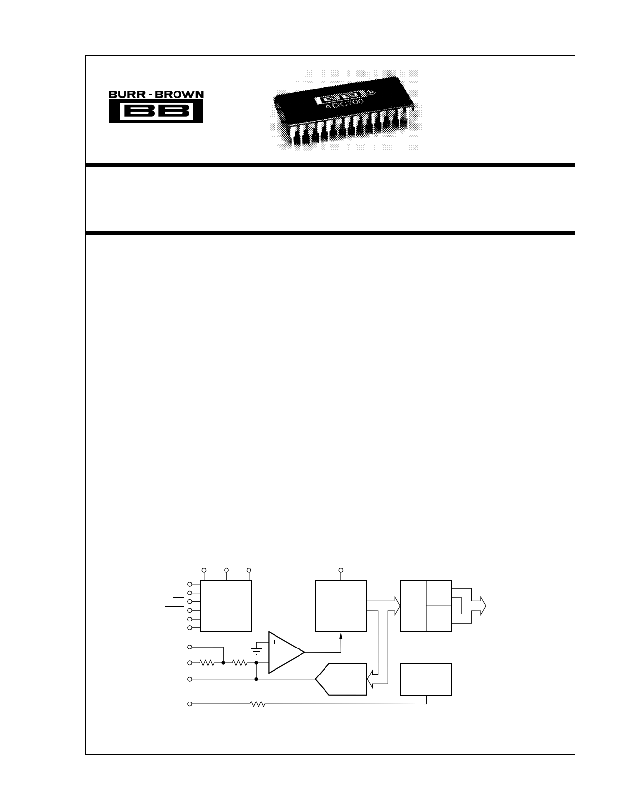
DESCRIPTION
AND OPERATING FEATURES
The ADC700 is a 16-bit resolution successive approxima-
tion A/D converter. Parallel digital data as well as serial data
is available. Several features have been included in the
ADC700 making it easier to interface with microprocessors
and/or serial data systems. Several analog input ranges are
available.
in the buffer register. The Data Ready flag goes low (“0”)
when the most significant byte (high byte) is read. If the
“old” word is not read, or if only the least significant byte
(low byte) is read, Data Ready is not reset. The next
conversion output will overwrite the data latch when the
conversion is complete. The Data Ready flag remains high.
Refer to timing diagrams in the Specifications section.
SERIAL DATA
Some of the key operating features are described here. More Sixteen-bit serial data output is available (pin 11) along with
detail is given in later sections of the data sheet. Refer to the a serial output strobe (pin 14). This serial data strobe is not
block diagram above.
the internal SAR clock but is a special strobe for serial data
consisting of 16 negative-going edges (during conversion)
RESET
The ADC700 has a Reset input that must be asserted upon
power-up or after a power interruption. This initializes the
occurring about 200ns after each serial data bit is valid. This
feature eases the interface to shift registers or through opto-
couplers for applications requiring galvanic isolation.
SAR, the output buffer register and Data Ready flag. Since
microprocessor systems already use a power-on reset circuit,
STATUS
the same system reset signal can be used to initialize the The familiar Status (or Busy) flag, present in successive
ADC700.
approximation A/D converters, is available (pin 13) and
indicates that a conversion is in progress. Status is valid
PARALLEL DATA
The parallel data output is available through an 8-bit port
with 3-state output drivers. High byte and low byte are
selected by HBEN (pin 10).
110ns after assertion of the convert command (WR low).
Status cannot be used as a sample-hold control because there
is not enough time for the sample-hold to settle to the
required error band before the ADC700 makes its first
conversion decision.
A buffer/latch is included between the successive approxi-
mation register (SAR) and the 3-state drivers. This feature
permits more flexible interface timing than is possible from
most successive approximation converters.
The “old” word can be read during the next conversion. A
Data Ready flag (pin 12) is asserted when a “new” word is
CHIP SELECT
CS (pin 9) selects the ADC700. No other functions can be
implemented unless CS is asserted. WR (pin 7) is the start-
of-conversion strobe. RD strobes each output data byte,
selected by HBEN (pin 10), to the 3-state drivers.
®
5 ADC700
5 Page 
Serial
Data
ADC700
Serial
Data
Strobe
V DD
ADC700
CS
WR
VDD To Interrupt
Status
FIGURE 11. Continuous Conversion Circuit Connection.
Reset
Isolation Barrier
FIGURE 10. Serial Data Output Providing Convenient
Isolation.
PIN DESIGNATION
CS (Pin 9)
WR (Pin 7)
RD (Pin 8)
HBEN (Pin 10)
Reset (Pin 6)
BTCEN (Pin 23)
DEFINITION
Chip Select
Write (Convert)
Read
High Byte Enable
“1” = Low Byte
“0” = High Byte
Reset
BTC Enable
TABLE III. Control Line Functions.
FUNCTION
Must be Low to either initiate a conversion or read output data.
Conversion begins after the High-to-Low transition.
Turns ON the three-state output drivers upon being asserted low.
Selects the MSB or the LSB for readout. Data Ready is cleared when HBEN is Low and RD is asserted.
Resets internal logic. Must be asserted after power-up or a power interruption clears Status and Data
Ready to Low.
Sets the output code to Binary Twos Complement (BTC) when Low. Output code is Bipolar Offset Binary
(BOB) when High.
CONTROL LINE
RESET
WR
RD HBEN CS
OPERATION
0 X X X X Reset converter logic. Status and Data Ready set Low.
1 X X X 1 No operation.
1 0 X X 0 Initiate conversion.
1 1 0 0 0 Places High Byte on output port. Clears Data Ready flag.
1 1 0 1 0 Placed Low Byte on output port. Does not clear Data Ready flag.
1 0 0 0 0 Initiates conversion and places High Byte or output port. Clears Data Ready.
1 0 0 1 0 Initiates conversion and places Low Byte on output port. Does not clear Data Ready flag.
NOTE: If a conversion command is asserted while a conversion is in progress, the command is ignored. If the conversion command remains asserted when a
conversion is finished, a new conversion will begin.
TABLE IV. Control Input Truth Table.
®
11 ADC700
11 Page | ||
| Páginas | Total 12 Páginas | |
| PDF Descargar | [ Datasheet ADC700BH.PDF ] | |
Hoja de datos destacado
| Número de pieza | Descripción | Fabricantes |
| ADC700BH | 16-Bit Resolution With Microprocessor Interface A/D CONVERTER | Burr-Brown Corporation |
| Número de pieza | Descripción | Fabricantes |
| SLA6805M | High Voltage 3 phase Motor Driver IC. |
Sanken |
| SDC1742 | 12- and 14-Bit Hybrid Synchro / Resolver-to-Digital Converters. |
Analog Devices |
|
DataSheet.es es una pagina web que funciona como un repositorio de manuales o hoja de datos de muchos de los productos más populares, |
| DataSheet.es | 2020 | Privacy Policy | Contacto | Buscar |