|
|
|
PDF ADC0819 Data sheet ( Hoja de datos )
| Número de pieza | ADC0819 | |
| Descripción | 8-Bit Serial I/O A/D Converter with 19-Channel Multiplexer | |
| Fabricantes | National Semiconductor | |
| Logotipo | ||
Hay una vista previa y un enlace de descarga de ADC0819 (archivo pdf) en la parte inferior de esta página. Total 16 Páginas | ||
|
No Preview Available !
ADC0819
OBSOLETE
September 26, 2009
8-Bit Serial I/O A/D Converter with 19-Channel Multiplexer
General Description
The ADC0819 is an 8-Bit successive approximation A/D con-
verter with simultaneous serial I/O. The serial input controls
an analog multiplexer which selects from 19 input channels
or an internal half scale test voltage.
An input sample-and-hold is implemented by a capacitive ref-
erence ladder and sampled data comparator. This allows the
input signal to vary during the conversion cycle.
Separate serial I/O and conversion clock inputs are provided
to facilitate the interface to various microprocessors.
Features
■ Separate asynchronous converter clock and serial data I/
O clock
■ 19-Channel multiplexer with 5-Bit serial address logic
■ Built-in sample and hold function
■ Ratiometric or absolute voltage referencing
■ No zero or full-scale adjust required
■ Internally addressable test voltage
■ 0V to 5V input range with single 5V power supply
■ TTL/MOS input/output compatible
■ 28-pin molded chip carrier or 28-pin molded DIP
Key Specifications
■ Resolution: 8-Bits
■ Total unadjusted error: ± ½ LSB and ± 1 LSB
■ Single supply: 5 VDC
■ Low Power: 15 mW
■ Conversion Time: 16 μs
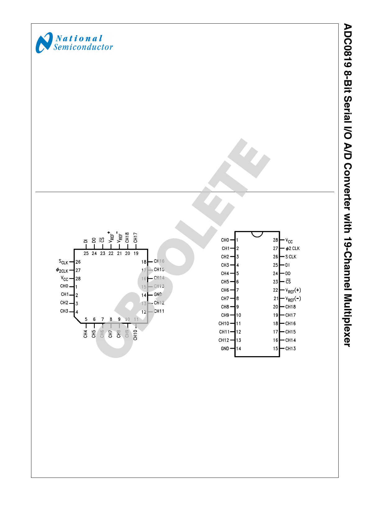
Connection Diagrams
Molded Chip Carrier (PCC) Package
Dual-In-Line Package
928701
Top View
Order Number ADC0819BCV, CCV
See NS Package Number V28A
928720
Top View
Order Number ADC0819BCN, CIN
See NS Package Number N28B
TRI-STATE® is a registered trademark of National Semiconductor Corporation.
© 2009 National Semiconductor Corporation 9287
9287 Version 2 Revision 4 Print Date/Time: 2009/08/26 15:48:51
www.national.com
1 page 
Parameter
tCA, Analog
Sampling Time
tRDO, Maximum DO Rise
Time
tFDO, Maximum DO Fall
Time
CIN, Maximum Input
Capacitance
Conditions
After Address Is Latched
CS = Low
RL=30 kΩ, “TRI-STATE” to “HIGH” State
CL=100 pF “LOW” to “HIGH” State
RL=30 kΩ, “TRI-STATE” to “LOW” State
CL=100 pF “HIGH” to “LOW” State
Analog Inputs, ANO–AN10 and VREF
All Others
Typical
(Note 6)
Tested
Limit
(Note 7)
75 150
150 300
75 150
150 300
11
5
Design
Limit
(Note 8)
3/SCLK+1 μs
150
300
150
300
55
15
Units
sec
ns
ns
pF
Note 1: Absolute Maximum Ratings indicate limits beyond which damage to the device may occur. DC and AC electrical specifications do not apply when operating
the device beyond its specified operating conditions.
Note 2: All voltages are measured with respect to ground.
Note 3: Under over voltage conditions (VIN<0V and VIN>VCC) the maximum input current at any one pin is ±5 mA. If the voltage at more than one pin exceeds
VCC + .3V the total package current must be limited to 20 mA. For example the maximum number of pins that can be over driven at the maximum current level
of ±5 mA is four.
Note 4: Total unadjusted error includes offset, full-scale, linearity, multiplexer, and hold step errors.
Note 5: Two on-chip diodes are tied to each analog input, which will forward-conduct for analog input voltages one diode drop below ground or one diode drop
greater than VCC supply. Be careful during testing at low VCClevels (4.5V), as high level analog inputs (5V) can cause this input diode to conduct, especially at
elevated temperatures, and cause errors for analog inputs near full-scale. The spec allows 50 mV forward bias of either diode. This means that as long as the
analog VIN does not exceed the supply voltage by more than 50 mV, the output code will be correct. To achieve an absolute 0 VDC to 5 VDC input voltage range
will therefore require a minimum supply voltage of 4.950 VDC over temperature variations, initial tolerance and loading.
Note 6: Typicals are at 25°C and represent most likely parametric norm.
Note 7: Tested Limits are guaranteed to National's AOQL (Average Outgoing Quality Level).
Note 8: Design Limits are guaranteed, but not 100% production tested. These limits are not used to calculate outgoing quality levels.
Note 9: Channel leakage current is measured after the channel selection.
Note 10: 1 count = VREF/256.
Note 11: Human body model; 100 pF discharged through a 1.5 kΩ resistor.
Test Circuits
Leakage Current
D0 Except “TRI-STATE”
928703
tTRI “TRI-STATE”
928704
928705
5
9287 Version 2 Revision 4 Print Date/Time: 2009/08/26 15:48:51
www.national.com
5 Page 
FIGURE 2.
928717
If CS goes high during the conversion sequence DO is tri-
stated, and the result is not affected so long as CS remains
high until the end of the conversion.
1.2 MULTIPLEXER ADDRESSING
The five bit mux address is shifted, MSB first, into DI. Input
data corresponds to the channel selected as shown in Table
1. Care should be taken not to send an address greater than
or equal to twenty four (11XXX) as this puts the A/D in a digital
testing mode. In this mode the analog inputs CH0 thru CH4
become digital outputs, for our use in production testing.
2.0 ANALOG INPUT
2.1 THE INPUT SAMPLE AND HOLD
The ADC0819's sample/hold capacitor is implemented in its
capacitive ladder structure. After the channel address is re-
ceived, the ladder is switched to sample the proper analog
input. This sampling mode is maintained for 1 μsec after the
eighth SCLK falling edge. The hold mode is initiated with the
start of the conversion process. An acquisition window of
3tSCLK+1 μsec is therefore available to allow the ladder ca-
Typical Applications
pacitance to settle to the analog input voltage. Any change in
the analog voltage before or after the acquisition window will
not effect the A/D conversion result.
In the most simple case, the ladder's acquisition time is de-
termined by the Ron (3K) of the multiplexer switches and the
total ladder capacitance (90 pF). These values yield an ac-
quisition time of about 2 μsec for a full scale reading. There-
fore the analog input must be stable for at least 2 μsec before
and 1 μsec after the eighth SCLK falling edge to ensure a
proper conversion. External input source resistance and ca-
pacitance will lengthen the acquisition time and should be
accounted for.
Other conventional sample and hold error specifications are
included in the error and timing specs of the A/D. The hold
step and gain error sample/hold specs are taken into account
in the ADC0819's total unadjusted error, while the hold set-
tling time is included in the A/D's max conversion time of 32
φ2 clock periods. The hold droop rate can be thought of as
being zero since an unlimited amount of time can pass be-
tween a conversion and the reading of data. However, once
the data is read it is lost and another conversion is started.
ADC0819-INS8048 INTERFACE
928718
11
9287 Version 2 Revision 4 Print Date/Time: 2009/08/26 15:48:51
www.national.com
11 Page | ||
| Páginas | Total 16 Páginas | |
| PDF Descargar | [ Datasheet ADC0819.PDF ] | |
Hoja de datos destacado
| Número de pieza | Descripción | Fabricantes |
| ADC08100 | 8-Bit/ 20 MSPS to 100 MSPS/ 1.3 mW/MSPS A/D Converter | National Semiconductor |
| ADC08100 | ADC08100 8-Bit 20 Msps to 100 Msps 1.3 mW/Msps A/D Converter (Rev. I) | Texas Instruments |
| ADC081000 | 1 GSPS A/D Converter | National Semiconductor |
| ADC081000 | ADC081000 High Performance Low Power 8-Bit 1 GSPS A/D Converter (Rev. G) | Texas Instruments |
| Número de pieza | Descripción | Fabricantes |
| SLA6805M | High Voltage 3 phase Motor Driver IC. |
Sanken |
| SDC1742 | 12- and 14-Bit Hybrid Synchro / Resolver-to-Digital Converters. |
Analog Devices |
|
DataSheet.es es una pagina web que funciona como un repositorio de manuales o hoja de datos de muchos de los productos más populares, |
| DataSheet.es | 2020 | Privacy Policy | Contacto | Buscar |