|
|
|
PDF AD9975 Data sheet ( Hoja de datos )
| Número de pieza | AD9975 | |
| Descripción | Broadband Modem Mixed-Signal Front End | |
| Fabricantes | Analog Devices | |
| Logotipo | ||
Hay una vista previa y un enlace de descarga de AD9975 (archivo pdf) en la parte inferior de esta página. Total 20 Páginas | ||
|
No Preview Available !
a
FEATURES
Low Cost, 3.3 V-CMOS, Mixed Signal, Front End
Converter for Broadband Modems
10-Bit D/A Converter (TxDAC+®)
50 MSPS Input Word Rate
2؋ Interpolating Low-Pass Transmit Filter
100 MSPS DAC Output Update Rate
Wide (21 MHz) Transmit Bandwidth
Power-Down Modes
10-Bit, 50 MSPS A/D Converter
Fourth Order LPF with Selectable Cutoff Frequency
Dual Mode Programmable Gain Amplifier
Internal Clock Multiplier (PLL)
Two Auxiliary Clock Outputs
48-Lead LQFP Package
APPLICATIONS
Powerline Networking
Home Phone Networking
Broadband Modem
Mixed-Signal Front End
AD9975
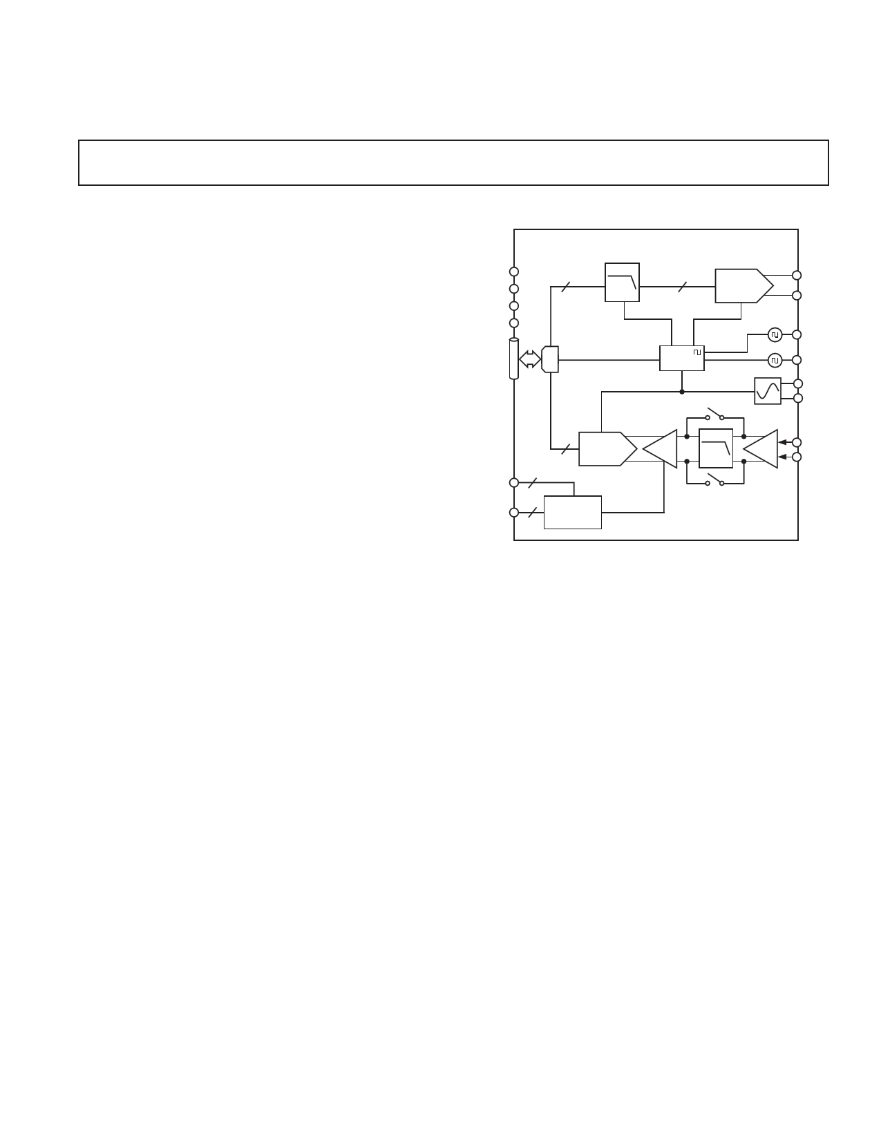
FUNCTIONAL BLOCK DIAGRAM
TXEN
RXEN
TXCLK
RXCLK
ADIO[9:0]
AD9975
10 K
10 TxDAC+
CLK-GEN
TX+
TX–
CLK1
CLK2
OSCIN
XTAL
10 ADC
AGC[2:0]
SPORT
3
3 REGISTER
CONTROL
PGA
LPF PGA RX+
RX–
GENERAL DESCRIPTION
The AD9975 is a single-supply, broadband modem, mixed
signal, front end (MxFE™) IC. The device contains a transmit
path interpolation filter and DAC and a receive path PGA,
LPF, and ADC required for a variety of broadband modem
applications. Also on-chip is a PLL clock multiplier that pro-
vides all required clocks from a single crystal or clock input.
The TxDAC+ uses a digital 2× interpolation low-pass filter to
oversample the transmit data and ease the complexity of analog
reconstruction filtering. The transmit path bandwidth is 21 MHz
when sampled at 100 MSPS. The 10-bit DAC provides differen-
tial current outputs. The DAC full-scale current can be adjusted
from 2 to 20 mA by a single resistor, providing 20 dB of additional
gain range.
The receive path consists of a PGA, LPF, and ADC. The program-
mable gain amplifier (PGA) has two modes of operation. One
mode allows programming through the serial port and provides a
gain range from –6 dB to +36 dB in 2 dB steps. The other mode
allows the gain to be controlled through an asynchronous 3-pin
port and offers a gain range from 0 dB to 48 dB in 8 dB steps
with the use of an external gain stage. The receive path LPF
cutoff frequency can be selected to either 12 MHz or 26 MHz.
The filter cutoff frequency can also be tuned or bypassed where
filter requirements differ. The 10-bit ADC uses a multistage
differential pipeline architecture to achieve excellent dynamic
performance with low power consumption.
The digital transmit and receive ports are multiplexed onto a
10-bit databus and have individual TX/RX clocks and TX/RX
enable lines. This interface connects directly to Homelug 1.0
PHY/MAC chips from Intellon and Conexant.
The AD9975 is available in a space-saving 48-lead LQFP pack-
age. The device is specified over the commercial (–40°C to
+85°C) temperature range.
TxDAC+ is a registered trademark and MxFE is a trademark of Analog Devices, Inc.
REV. 0
Information furnished by Analog Devices is believed to be accurate and
reliable. However, no responsibility is assumed by Analog Devices for its
use, nor for any infringements of patents or other rights of third parties that
may result from its use. No license is granted by implication or otherwise
under any patent or patent rights of Analog Devices.
One Technology Way, P.O. Box 9106, Norwood, MA 02062-9106, U.S.A.
Tel: 781/329-4700
www.analog.com
Fax: 781/326-8703
© Analog Devices, Inc., 2002
1 page 
Model
AD9975ABST
AD9975ABSTEB
AD9975ABSTRL
ORDERING GUIDE
Temperature Range
–40ºC to +85ºC
–40ºC to +85ºC
–40ºC to +85ºC
Package Description
48-Lead LQFP
AD9975 EVAL Board
AD9975ABST Reel
AD9975
Package Option
ST-48
CAUTION
ESD (electrostatic discharge) sensitive device. Electrostatic charges as high as 4000 V readily
accumulate on the human body and test equipment and can discharge without detection. Although the
AD9975 features proprietary ESD protection circuitry, permanent damage may occur on devices
subjected to high energy electrostatic discharges. Therefore, proper ESD precautions are recommended
to avoid performance degradation or loss of functionality.
WARNING!
ESD SENSITIVE DEVICE
PIN FUNCTION DESCRIPTION
Pin No. Mnemonic Function
1
2
3
4
5, 38, 47
6, 9, 39, 42,
43, 46
7
8
10
11
12
13
14
15–17
18
19–28
29
30
31
32
33
34
35
36
37
40, 41
44
45
48
OSC IN
SENABLE
SCLK
SDATA
AVDD
AVSS
Tx+
Tx–
FS ADJ
REFIO
CLKVDD
DVSS
DVDD
AGC[2:0]
CLKOUT1
ADIO[9:0]
RXEN
TXEN
TXCLK
RXCLK
CLKOUT2
RXBOOST/
SDO
DRVDD
DRVSS
RESET
REFB, REFT
Rx+
Rx–
XTAL
Crystal Oscillator Inverter Input
Serial Bus Enable Input
Serial Bus Clock Input
Serial Bus Data I/O
Analog 3.3 V Power Supply
Analog Ground
Transmit DAC + Output
Transmit DAC – Output
DAC Full-Scale Output Current
Adjust with External Resistor
DAC Band Gap Decoupling Node
Power Supply for CLKOUT1
Digital Ground
Digital 3.3 V Power Supply
AGC Control Inputs
Auxiliary Clock Output
Digital Data I/O Port
ADIO Direction Control Input
TX Path Enable
ADIO Sample Clock Input
ADIO Request Clock Input
Auxiliary Clock Output
External Gain Control Output/
Serial Data Output
Digital I/O 3.3 V Power Supply
Digital I/O Ground
Reset Input
ADC Reference Decoupling Node
Receive Path + Input
Receive Path – Input
Crystal Oscillator Inverter Output
PIN CONFIGURATION
OSC IN 1
SENABLE 2
SCLK 3
SDATA 4
AVDD 5
AVSS 6
TX+ 7
TX– 8
AVSS 9
FS ADJ 10
REFIO 11
CLKVDD 12
AD9975
48-PIN LQFP
TOP VIEW
(Not to Scale)
36 DRVSS
35 DRVDD
34 RXBOOST/SDO
33 CLKOUT2
32 RXCLK
31 TXCLK
30 TXEN
29 RXEN
28 ADIO0
27 ADIO1
26 ADIO2
25 ADIO3
REV. 0
–5–
5 Page 
58
57
56
55
54
53
52
51
50
0 2 4 6 8 10 12 14 16 18 20
FIN – MHz
TPC 25. Rx Path SNR vs. FIN, FADC = 50 MHz,
Gain = –6 dB, Rx LPF Bypassed
AD9975
–50
–55
–60
–65
–70
–75
0 2 4 6 8 10 12 14 16 18 20
FIN – MHz
TPC 26. Rx Path THD vs. FIN, FADC = 50 MHz,
Gain = –6 dB, Rx LPF Bypassed
REV. 0
–11–
11 Page | ||
| Páginas | Total 20 Páginas | |
| PDF Descargar | [ Datasheet AD9975.PDF ] | |
Hoja de datos destacado
| Número de pieza | Descripción | Fabricantes |
| AD9970 | 14-Bit CCD Signal Processor | Analog Devices |
| AD9971 | 12-Bit CCD Signal Processor | Analog Devices |
| AD9972 | CCD Signal Processor | Analog Devices |
| AD9973 | 14-Bit CCD Signal Processor | Analog Devices |
| Número de pieza | Descripción | Fabricantes |
| SLA6805M | High Voltage 3 phase Motor Driver IC. |
Sanken |
| SDC1742 | 12- and 14-Bit Hybrid Synchro / Resolver-to-Digital Converters. |
Analog Devices |
|
DataSheet.es es una pagina web que funciona como un repositorio de manuales o hoja de datos de muchos de los productos más populares, |
| DataSheet.es | 2020 | Privacy Policy | Contacto | Buscar |