|
|
|
PDF AD9887 Data sheet ( Hoja de datos )
| Número de pieza | AD9887 | |
| Descripción | Dual Interface for Flat Panel Displays | |
| Fabricantes | Analog Devices | |
| Logotipo | ||
Hay una vista previa y un enlace de descarga de AD9887 (archivo pdf) en la parte inferior de esta página. Total 30 Páginas | ||
|
No Preview Available !
a
Dual Interface for
Flat Panel Displays
AD9887
FEATURES
Analog Interface
140 MSPS Maximum Conversion Rate
330 MHz Analog Bandwidth
0.5 V to 1.0 V Analog Input Range
500 ps p-p PLL Clock Jitter at 140 MSPS
3.3 V Power Supply
Full Sync Processing
Midscale Clamp
4:2:2 Output Format Mode
Digital (DVI 1.0 Compatible) Interface
112 MHz Operation (1 Pixel/Clock Mode)
High Skew Tolerance of One Full Input Clock
Sync Detect for “Hot Plugging”
APPLICATIONS
RGB Graphics Processing
LCD Monitors and Projectors
Plasma Display Panels
Scan Converters
Micro Displays
Digital TV
GENERAL DESCRIPTION
The AD9887 offers designers the flexibility of a dual analog and
digital interface for flat panel displays (FPDs) on a single chip.
Both interfaces are optimized for excellent image quality supporting
display resolutions up to SXGA (1280 × 1024 at 75 Hz). Either the
analog or the digital interface can be selected by the user.
Analog Interface
For ease of design and to minimize cost, the AD9887 is a fully
integrated interface solution for FPDs. The AD9887 includes an
analog interface with a 140 MHz triple ADC with internal 1.25 V
reference, PLL to generate a pixel clock from HSYNC, program-
mable gain, offset, and clamp control. The user provides only a
3.3 V power supply, analog input, and HSYNC. Three-state
CMOS outputs may be powered from 2.5 V to 3.3 V.
The AD9887’s on-chip PLL generates a pixel clock from HSYNC.
Pixel clock output frequencies range from 12 MHz to 140 MHz.
PLL clock jitter is 500 ps p-p typical at 140 MSPS. When a
COAST signal is presented, the PLL maintains its output fre-
quency in the absence of HSYNC. A sampling phase adjustment is
provided. Data, HSYNC and Clock output phase relationships are
maintained. The PLL can be disabled and an external clock input
provided as the pixel clock. The AD9887 also offers full sync pro-
cessing for composite sync and sync-on-green applications.
A clamp signal is generated internally or may be provided by
the user through the CLAMP input pin. The analog interface
is fully programmable via a 2-wire serial interface.
REV. 0
Information furnished by Analog Devices is believed to be accurate and
reliable. However, no responsibility is assumed by Analog Devices for its
use, nor for any infringements of patents or other rights of third parties that
may result from its use. No license is granted by implication or otherwise
under any patent or patent rights of Analog Devices.
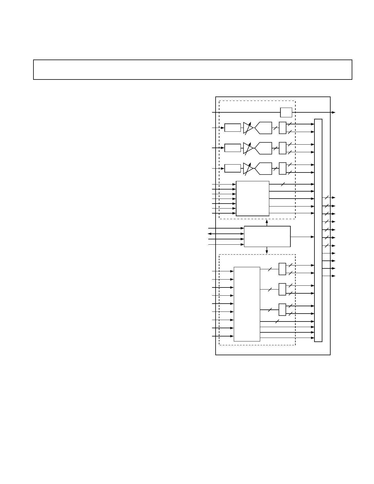
FUNCTIONAL BLOCK DIAGRAM
REFIN
RAIN
GAIN
BAIN
HSYNC
VSYNC
COAST
CLAMP
CKINV
CKEXT
FILT
SCL
SDA
A1
A0
Rx0+
Rx0–
Rx1+
Rx1–
Rx2+
Rx2–
RxC+
RxC–
RTERM
ANALOG
INTERFACE
CLAMP
REF
8
A/D
8 ROUTA
8 ROUTB
CLAMP
8
A/D
8 GOUTA
8 GOUTB
CLAMP
8
A/D
8 BOUTA
8 BOUTB
SYNC
PROCESSING
AND CLOCK
GENERATION
2
SERIAL REGISTER
AND
POWER MANAGEMENT
DATACK
HSOUT
VSOUT
8
SOGOUT
SCDT
8
8
M8
U
X
8
E
S
8
2
DIGITAL
INTERFACE
DVI
RECEIVER
8
8
8
2
8 ROUTA
8 ROUTB
8 GOUTA
8 GOUTB
8 BOUTA
8 BOUTB
DATACK
DE
HSYNC
VSYNC
REFOUT
ROUTA
ROUTB
GOUTA
GOUTB
BOUTA
BOUTB
DATACK
HSOUT
VSOUT
SOGOUT
DE
AD9887
Digital Interface
The AD9887 contains a Digital Video Interface (DVI 1.0) compat-
ible receiver. This receiver supports displays ranging from VGA
to SXGA (25 MHz to 112 MHz). The receiver operates with
true color (24-bit) panels in 1 or 2 pixel(s)/clock mode, and also
features an intrapair skew tolerance up to one full clock cycle.
Fabricated in an advanced CMOS process, the AD9887 is pro-
vided in a 160-lead MQFP surface mount plastic package and is
specified over the 0°C to 70°C temperature range.
One Technology Way, P.O. Box 9106, Norwood, MA 02062-9106, U.S.A.
Tel: 781/329-4700
www.analog.com
Fax: 781/326-8703
© Analog Devices, Inc., 2001
1 page 
AD9887
Parameter
AC SPECIFICATIONS (continued)
High-to-Low Transition Time for DATACK (DHLT)
Clock to Data Skew, tSKEW
Duty Cycle, tDCYCLE
Conditions
Output Drive = High; CL =10 pF
Output Drive = Med; CL = 7 pF
Output Drive = Low; CL = 5 pF
Test
AD9887KS
Level Min Typ Max
IV
IV
IV
IV –0.5
IV 45
1.4
1.7
2.1
+2.0
55
DATACK Frequency (FCIP) (1 Pixel/Clock)
DATACK Frequency (FCIP) (2 Pixels/Clock)
NOTES
1The typical pattern contains a gray scale area, Output Drive = High.
2The worst-case pattern contains a black and white checkerboard pattern, Output Drive = High.
3The setup and hold times with respect to the DATACK rising edge are the same as the falling edge.
41 Pixel/clock mode, DATACK and DATACK Load = 10 pF, Data Load = 5 pF.
VI 20
IV 10
112
56
Unit
ns
ns
ns
ns
% of
Period
High
MHz
MHz
ABSOLUTE MAXIMUM RATINGS*
VD . . . . . . . . . . . . . . . . . . . . . . . . . . . . . . . . . . . . . . . . . 3.6 V
VDD . . . . . . . . . . . . . . . . . . . . . . . . . . . . . . . . . . . . . . . . 3.6 V
Analog Inputs . . . . . . . . . . . . . . . . . . . . . . . . . . . VD to 0.0 V
VREF IN . . . . . . . . . . . . . . . . . . . . . . . . . . . . . . . VD to 0.0 V
Digital Inputs . . . . . . . . . . . . . . . . . . . . . . . . . . . 5 V to 0.0 V
Digital Output Current . . . . . . . . . . . . . . . . . . . . . . . . 20 mA
Operating Temperature . . . . . . . . . . . . . . . . . –25°C to +85°C
Storage Temperature . . . . . . . . . . . . . . . . . . –65°C to +150°C
Maximum Junction Temperature . . . . . . . . . . . . . . . . 150°C
Maximum Case Temperature . . . . . . . . . . . . . . . . . . . 150°C
*Stresses above those listed under Absolute Maximum Ratings may cause perma-
nent damage to the device. This is a stress rating only; functional operation of the
device at these or any other conditions outside of those indicated in the operation
sections of this specification is not implied. Exposure to absolute maximum ratings
for extended periods may affect device reliability.
EXPLANATION OF TEST LEVELS
Test Level
I
II
III
IV
V
VI
Explanation
100% production tested.
100% production tested at 25°C and sample
tested at specified temperatures.
Sample tested only.
Parameter is guaranteed by design and charac-
terization testing.
Parameter is a typical value only.
100% production tested at 25°C; guaranteed
by design and characterization testing.
Model
AD9887KS-140
AD9887KS-100
AD9887/PCB
ORDERING GUIDE
Temperature
Range
0°C to 70°C
0°C to 70°C
25°C
Package
Description
Plastic Quad Flatpack
Plastic Quad Flatpack
Evaluation Board
Package
Option
S-160
S-160
CAUTION
ESD (electrostatic discharge) sensitive device. Electrostatic charges as high as 4000 V readily
accumulate on the human body and test equipment and can discharge without detection. Although
the AD9887 features proprietary ESD protection circuitry, permanent damage may occur on
devices subjected to high-energy electrostatic discharges. Therefore, proper ESD precautions are
recommended to avoid performance degradation or loss of functionality.
WARNING!
ESD SENSITIVE DEVICE
REV. 0
–5–
5 Page 
AD9887
Either or both signals may be used, depend-
ing on the timing mode and interface design
employed.
HSOUT
Horizontal Sync Output
A reconstructed and phase-aligned version of
the Hsync input. Both the polarity and dura-
tion of this output can be programmed via
serial bus registers.
By maintaining alignment with DATACK,
DATACK, and Data, data timing with
respect to horizontal sync can always be
determined.
SOGOUT
Sync-On-Green Slicer Output
This pin can be programmed to output
either the output from the Sync-On-Green
slicer comparator or an unprocessed but
delayed version of the HSYNC input. See
the Sync Block Diagram to view how this
pin is connected.
(Note: The output from this pin is the sliced
SOG, without additional processing from the
AD9887.)
Analog Interface
REFOUT
Internal Reference Output
Output from the internal 1.25 V bandgap refer-
ence. This output is intended to drive relatively
light loads. It can drive the AD9887 Reference
Input directly, but should be externally buff-
ered if it is used to drive other loads as well.
The absolute accuracy of this output is ± 4%,
and the temperature coefficient is ± 50 ppm,
which is adequate for most AD9887 appli-
cations. If higher accuracy is required, an
external reference may be employed instead.
If an external reference is used, connect this
pin to ground through a 0.1 µF capacitor.
REFIN
Reference Input
The reference input accepts the master refer-
ence voltage for all AD9887 internal circuitry
(1.25 V ± 10%). It may be driven directly by
the REFOUT pin. Its high impedance pre-
sents a very light load to the reference source.
This pin should always be bypassed to Ground
with a 0.1 µF capacitor.
FILT
External Filter Connection
For proper operation, the pixel clock genera-
tor PLL requires an external filter. Connect
the filter shown Figure 7 to this pin. For
optimal performance, minimize noise and
parasitics on this node.
Power Supply
VD
VDD
PVD
GND
Main Power Supply
These pins supply power to the main elements
of the circuit. It should be filtered to be as
quiet as possible.
Digital Output Power Supply
These supply pins are identified separately
from the VD pins so special care can be taken
to minimize output noise transferred into the
sensitive analog circuitry.
If the AD9887 is interfacing with lower-
voltage logic, VDD may be connected to a
lower supply voltage (as low as 2.2 V) for
compatibility.
Clock Generator Power Supply
The most sensitive portion of the AD9887 is
the clock generation circuitry. These pins
provide power to the clock PLL and help the
user design for optimal performance. The
designer should provide noise-free power to
these pins.
Ground
The ground return for all circuitry on chip.
It is recommended that the application circuit
board have a single, solid ground plane.
THEORY OF OPERATION (INTERFACE DETECTION)
Active Interface Detection and Selection
The AD9887 includes circuitry to detect whether or not an
interface is active.
For detecting the analog interface, the circuitry monitors the
presence of HSYNC, VSYNC, and Sync-on-Green. The result of
the detection circuitry can be read from the 2-wire serial inter-
face bus at address 11H Bits 7, 6, and 5 respectively. If one of
these sync signals disappears, the maximum time it takes for the
circuitry to detect it is 100 ms.
There are two stages for detecting the digital interface. The first
stage searches for the presence of the digital interface clock.
The circuitry for detecting the digital interface clock is active
even when the digital interface is powered down. The result of
this detection stage can be read from the 2-wire serial interface
bus at address 11H Bit 4. If the clock disappears, the maximum
time it takes for the circuitry to detect it is 100 ms. The second
stage attempts to detect DE on the digital interface. Detection is
accomplished when 32 DEs have been counted. DE can only be
detected when the digital interface is powered up, so it is not
always active. The DE detection circuitry is one of the logic
inputs used to set the SyncDT output pin (Pin 136). The logic
for the SyncDT pin is [DE detect] OR [HSYNC detect].
There is an override for the automatic interface selection. It is
the AIO bit (Active Interface Override). When the AIO bit is set
to Logic 0, the automatic circuitry will be used. When the AIO
bit is set to Logic 1, the AIS bit will be used to determine the
active interface rather than the automatic circuitry.
REV. 0
–11–
11 Page | ||
| Páginas | Total 30 Páginas | |
| PDF Descargar | [ Datasheet AD9887.PDF ] | |
Hoja de datos destacado
| Número de pieza | Descripción | Fabricantes |
| AD9880 | Analog/HDMI Dual Display Interface | Analog Devices |
| AD9882 | Dual Interface for Flat Panel Displays | Analog Devices |
| AD9882A | Dual Interface | Analog Devices |
| AD9883 | 110 MSPS Analog Interface for Flat Panel Displays | Analog Devices |
| Número de pieza | Descripción | Fabricantes |
| SLA6805M | High Voltage 3 phase Motor Driver IC. |
Sanken |
| SDC1742 | 12- and 14-Bit Hybrid Synchro / Resolver-to-Digital Converters. |
Analog Devices |
|
DataSheet.es es una pagina web que funciona como un repositorio de manuales o hoja de datos de muchos de los productos más populares, |
| DataSheet.es | 2020 | Privacy Policy | Contacto | Buscar |