|
|
|
PDF AD9845A Data sheet ( Hoja de datos )
| Número de pieza | AD9845A | |
| Descripción | Complete 12-Bit 30 MSPS CCD Signal Processor | |
| Fabricantes | Analog Devices | |
| Logotipo | ||
Hay una vista previa y un enlace de descarga de AD9845A (archivo pdf) en la parte inferior de esta página. Total 22 Páginas | ||
|
No Preview Available !
a
FEATURES
30 MSPS Correlated Double Sampler (CDS)
4 dB ؎ 6 dB 6-Bit Pixel Gain Amplifier (PxGA®)
2 dB to 36 dB 10-Bit Variable Gain Amplifier (VGA)
Low Noise Clamp Circuits
Analog Preblanking Function
12-Bit 30 MSPS A/D Converter
Auxiliary Inputs with VGA and Input Clamp
3-Wire Serial Digital Interface
3 V Single Supply Operation
Low Power: 140 mW @ 3 V Supply
48-Lead LQFP Package
APPLICATIONS
Digital Still Cameras
Digital Video Camcorders
Industrial Imaging
Complete 12-Bit 30 MSPS
CCD Signal Processor
AD9845A
PRODUCT DESCRIPTION
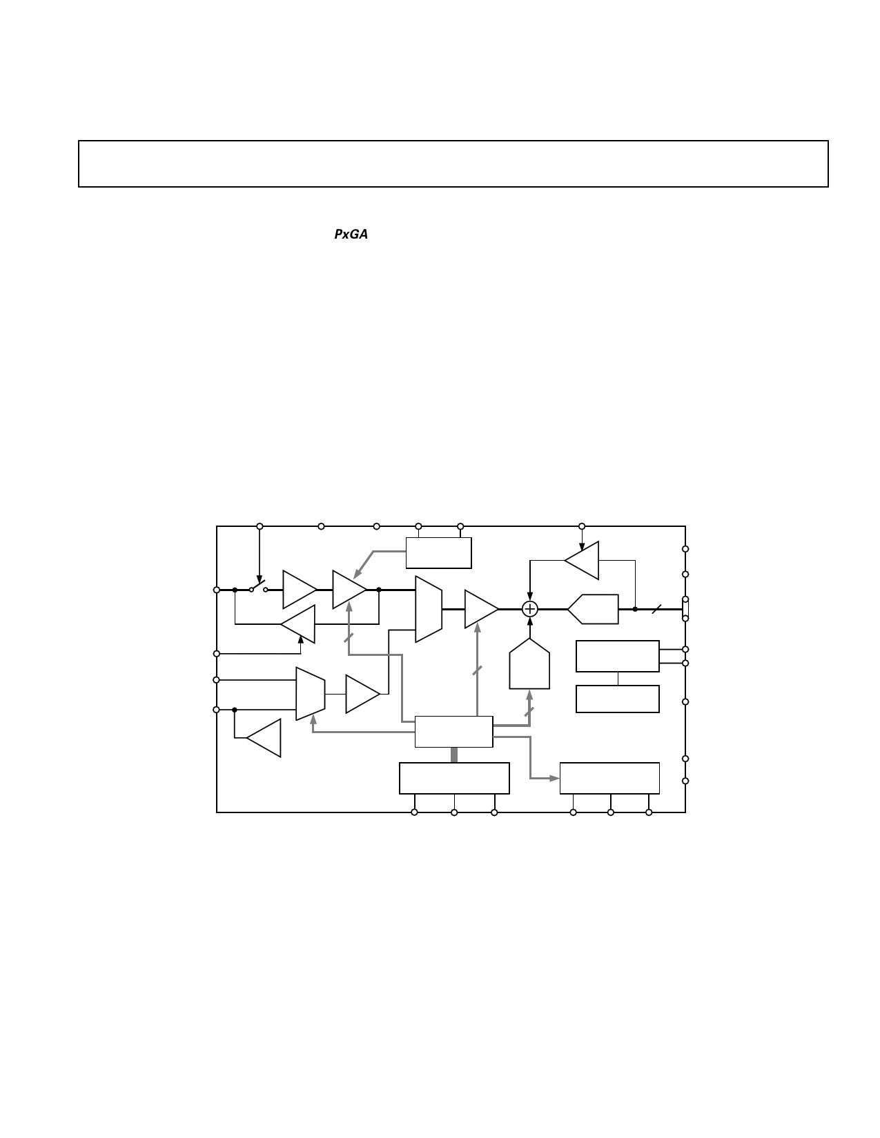
The AD9845A is a complete analog signal processor for CCD
applications. It features a 30 MHz single-channel architecture
designed to sample and condition the outputs of interlaced and
progressive scan area CCD arrays. The AD9845A’s signal chain
consists of an input clamp, correlated double sampler (CDS),
Pixel Gain Amplifier (PxGA), digitally controlled variable gain
amplifier (VGA), black level clamp, and a 12-bit A/D converter.
Additional input modes are provided for processing analog
video signals.
The internal registers are programmed through a 3-wire
serial digital interface. Programmable features include gain
adjustment, black level adjustment, input configuration, and
power-down modes.
The AD9845A operates from a single 3 V power supply, typi-
cally dissipates 140 mW, and is packaged in a 48-lead LQFP.
CCDIN
CLPDM
AUX1IN
AUX2IN
PBLK
FUNCTIONAL BLOCK DIAGRAM
AVDD
AVSS
HD
VD
CLPOB
4dB ؎ 6dB
CDS
PxGA
CLP
6
2:1
MUX
BUF
CLP
COLOR
STEERING
2:1
MUX
2dB~36dB
VGA
CLP
ADC
12
OFFSET
10 DAC
CONTROL
REGISTERS
8
BANDGAP
REFERENCE
INTERNAL
BIAS
AD9845A
DIGITAL
INTERFACE
INTERNAL
TIMING
DRVDD
DRVSS
DOUT
VRT
VRB
CML
DVDD
DVSS
SL SCK SDATA
SHP SHD DATACLK
PxGA is a registered trademark of Analog Devices, Inc.
REV. 0
Information furnished by Analog Devices is believed to be accurate and
reliable. However, no responsibility is assumed by Analog Devices for its
use, nor for any infringements of patents or other rights of third parties
which may result from its use. No license is granted by implication or
otherwise under any patent or patent rights of Analog Devices.
One Technology Way, P.O. Box 9106, Norwood, MA 02062-9106, U.S.A.
Tel: 781/329-4700 World Wide Web Site: http://www.analog.com
Fax: 781/326-8703
© Analog Devices, Inc., 2001
1 page 
AD9845A
TIMING SPECIFICATIONS (CL = 20 pF, fSAMP = 30 MHz, CCD-Mode Timing in Figures 10 and 11, AUX-Mode Timing in Figure 7.
Serial Timing in Figures 26–29.)
Parameter
Symbol
Min
Typ Max
Unit
SAMPLE CLOCKS
DATACLK, SHP, SHD Clock Period
DATACLK Hi/Low Pulsewidth
SHP Pulsewidth
SHD Pulsewidth
CLPDM Pulsewidth
CLPOB Pulsewidth1
SHP Rising Edge to SHD Falling Edge
SHP Rising Edge to SHD Rising Edge
Internal Clock Delay
Inhibited Clock Period
DATA OUTPUTS
Output Delay
Output Hold Time
Pipeline Delay
tCONV
tADC
tSHP
tSHD
tCDM
tCOB
tS1
tS2
tID
tINH
tOD
tH
32
13
5
5
4
2
0
13
10
7.0
33
16.7
8.3
8.3
10
20
8.3
16.7
3.0
14.5 16
7.6
9
ns
ns
ns
ns
Pixels
Pixels
ns
ns
ns
ns
ns
ns
Cycles
SERIAL INTERFACE
Maximum SCK Frequency
SL to SCK Setup Time
SCK to SL Hold Time
SDATA Valid to SCK Rising Edge Setup
SCK Falling Edge to SDATA Valid Hold
SCK Falling Edge to SDATA Valid Read
fSCLK
tLS
tLH
tDS
tDH
tDV
10
10
10
10
10
10
NOTES
1Minimum CLPOB pulsewidth is for functional operation only. Wider typical pulses are recommended to achieve low noise clamp performance.
Specifications subject to change without notice.
MHz
ns
ns
ns
ns
ns
ABSOLUTE MAXIMUM RATINGS
Parameter
With
Respect
To Min Max
Unit
AVDD1, AVDD2
AVSS –0.3 +3.9
V
DVDD1, DVDD2
DVSS –0.3 +3.9
V
DRVDD
DRVSS –0.3 +3.9
V
Digital Outputs
DRVSS –0.3 DRVDD + 0.3 V
SHP, SHD, DATACLK DVSS –0.3 DVDD + 0.3 V
CLPOB, CLPDM, PBLK DVSS –0.3 DVDD + 0.3 V
SCK, SL, SDATA
DVSS –0.3 DVDD + 0.3 V
VRT, VRB, CMLEVEL AVSS –0.3 AVDD + 0.3 V
BYP1-4, CCDIN
AVSS –0.3 AVDD + 0.3 V
Junction Temperature
150 °C
Lead Temperature
300 °C
(10 sec)
ORDERING GUIDE
Model
Temperature
Range
AD9845AJST –20°C to +85°C
Package
Description
Thin Plastic
Quad Flatpack
(LQFP)
Package
Option
ST-48
THERMAL CHARACTERISTICS
Thermal Resistance
48-Lead LQFP Package
θJA = 92°C
CAUTION
ESD (electrostatic discharge) sensitive device. Electrostatic charges as high as 4000 V readily
accumulate on the human body and test equipment and can discharge without detection. Although
the AD9845A features proprietary ESD protection circuitry, permanent damage may occur on
devices subjected to high-energy electrostatic discharges. Therefore, proper ESD precautions are
recommended to avoid performance degradation or loss of functionality.
WARNING!
ESD SENSITIVE DEVICE
REV. 0
–5–
5 Page 
VD
012012012...
LINE n
...01201
012012012...
LINE n+1
HD
NOTE: 0 = GAIN0, 1 = GAIN1, 2 = GAIN2
Figure 12. PxGA Mode 3 (3-Color) Frame/Line Gain Register Sequence
AD9845A
VD
HD
SHP
5 PIXEL MIN
5 PIXEL MIN
3ns MIN
PxGA GAIN
GAINX GAIN0
GAIN1 GAIN2 GAIN0
NOTES:
1. BOTH VD AND HD ARE INTERNALLY UPDATED AT SHP RISING EDGES.
2. EVERY HD RISING EDGE WITH A PREVIOUS VD RISING EDGE WILL RESET TO 012012.
Figure 13. PxGA Mode 3 (3-Color) Detailed Timing
GAINX
GAIN0
GAIN1
VD
01230123012...
LINE n
...01230
012301230123...
LINE n+1
HD
NOTE: 0 = GAIN0, 1 = GAIN1, 2 = GAIN2, 3 = GAIN3
Figure 14. PxGA Mode 4 (4-Color) Frame/Line Gain Register Sequence
VD
HD
SHP
5 PIXEL MIN
5 PIXEL MIN
3ns MIN
PxGA GAIN
GAINX GAIN0
GAIN1 GAIN2
GAIN0
NOTES:
1. BOTH VD AND HD ARE INTERNALLY UPDATED AT SHP RISING EDGES.
2. EVERY HD RISING EDGE WITH A PREVIOUS VD RISING EDGE WILL RESET TO 01230123.
Figure 15. PxGA Mode 4 (4-Color) Detailed Timing
GAINX
GAIN0
GAIN1
REV. 0
–11–
11 Page | ||
| Páginas | Total 22 Páginas | |
| PDF Descargar | [ Datasheet AD9845A.PDF ] | |
Hoja de datos destacado
| Número de pieza | Descripción | Fabricantes |
| AD9845A | Complete 12-Bit 30 MSPS CCD Signal Processor | Analog Devices |
| AD9845B | Complete 12-Bit 30 MSPS CCD Signal Processor | Analog Devices |
| Número de pieza | Descripción | Fabricantes |
| SLA6805M | High Voltage 3 phase Motor Driver IC. |
Sanken |
| SDC1742 | 12- and 14-Bit Hybrid Synchro / Resolver-to-Digital Converters. |
Analog Devices |
|
DataSheet.es es una pagina web que funciona como un repositorio de manuales o hoja de datos de muchos de los productos más populares, |
| DataSheet.es | 2020 | Privacy Policy | Contacto | Buscar |