|
|
|
PDF AD2S90 Data sheet ( Hoja de datos )
| Número de pieza | AD2S90 | |
| Descripción | Complete 12-Bit Resolver-to-Digital Converter | |
| Fabricantes | Analog Devices | |
| Logotipo | ||
Hay una vista previa y un enlace de descarga de AD2S90 (archivo pdf) en la parte inferior de esta página. Total 12 Páginas | ||
|
No Preview Available !
a
FEATURES
Complete Monolithic Resolver-to-Digital Converter
Incremental Encoder Emulation (1024-Line)
Absolute Serial Data (12-Bit)
Differential Inputs
12-Bit Resolution
Industrial Temperature Range
20-Lead PLCC
Low Power (50 mW)
APPLICATIONS
Industrial Motor Control
Servo Motor Control
Industrial Gauging
Encoder Emulation
Automotive Motion Sensing and Control
Factory Automation
Limit Switching
Low Cost, Complete 12-Bit
Resolver-to-Digital Converter
SIN
SIN LO
COS
COS LO
NMC
A
B
NM
CS
SCLK
DATA
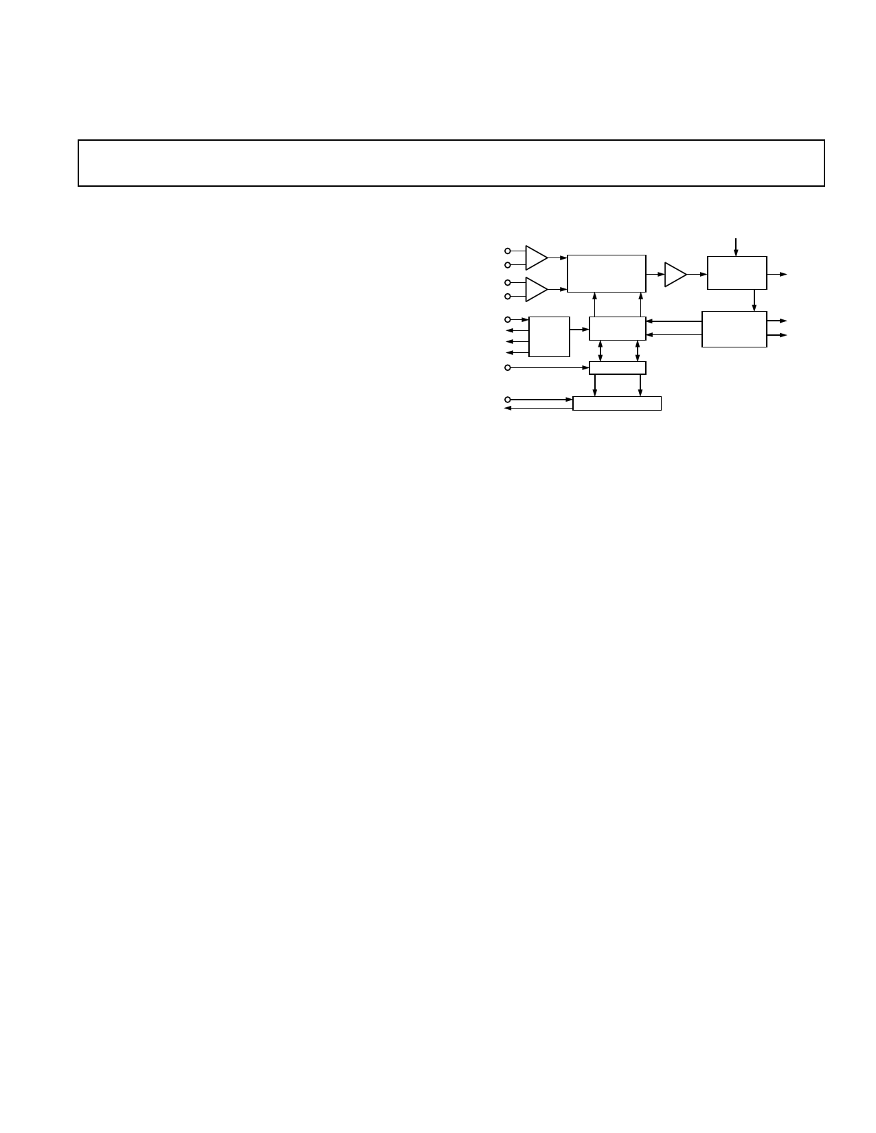
AD2S90
FUNCTIONAL BLOCK DIAGRAM
REF
HIGH ACCURACY
ANGLE
SIN COS
MULTIPLIER
DECODE
LOGIC
DIGITAL
ANGLE
UP-DOWN
COUNTER
SIN ( – )
P.S.D. AND
FREQUENCY
SHAPING
ERROR
AMPLIFIER
VEL
U/D
CLK
CLKOUT
HIGH
DYNAMIC
RANGE V.C.O. DIR
LATCH
SERIAL INTERFACE
GENERAL DESCRIPTION
The AD2S90 is a complete 12-bit resolution tracking resolver-
to-digital converter. No external components are required to
operate the device.
The converter accepts 2 V rms ± 10% input signals in the range
3 kHz–20 kHz on the SIN, COS and REF inputs. A Type II
servo loop is employed to track the inputs and convert the input
SIN and COS information into a digital representation of the
input angle. The bandwidth of the converter is set internally at
1 kHz within the tolerances of the device. The guaranteed maxi-
mum tracking rate is 500 rps.
Angular position output information is available in two forms,
absolute serial binary and incremental A quad B.
The absolute serial binary output is 12-bit (1 in 4096). The data
output pin is high impedance when Chip Select CS is logic HI.
This allows the connection of multiple converters onto a com-
mon bus. Absolute angular information in serial pure binary
form is accessed by CS followed by the application of an exter-
nal clock (SCLK) with a maximum rate of 2 MHz.
The encoder emulation outputs A, B and NM continuously
produce signals equivalent to a 1024 line encoder. When de-
coded this corresponds to 12 bits of resolution. Three common
north marker pulsewidths are selected via a single pin (NMC).
An analog velocity output signal provides a representation of
velocity from a rotating resolver shaft traveling in either a clock-
wise or counterclockwise direction.
The AD2S90 operates on ± 5 V dc ± 5% power supplies and is
fabricated on Analog Devices’ Linear Compatible CMOS pro-
cess (LC2MOS). LC2MOS is a mixed technology process that
combines precision bipolar circuits with low power CMOS logic
circuits.
PRODUCT HIGHLIGHTS
Complete Resolver-Digital Interface. The AD2S90 provides
the complete solution for digitizing resolver signals (12-bit reso-
lution) without the need for external components.
Dual Format Position Data. Incremental encoder emulation
in standard A QUAD B format with selectable North Marker
width. Absolute serial 12-bit angular binary position data
accessed via simple 3-wire interface.
Single High Accuracy Grade in Low Cost Package. ±10.6 arc
minutes of angular accuracy available in a 20-lead PLCC.
Low Power. Typically 50 mW power consumption.
REV. D
Information furnished by Analog Devices is believed to be accurate and
reliable. However, no responsibility is assumed by Analog Devices for its
use, nor for any infringements of patents or other rights of third parties
which may result from its use. No license is granted by implication or
otherwise under any patent or patent rights of Analog Devices.
One Technology Way, P.O. Box 9106, Norwood, MA 02062-9106, U.S.A.
Tel: 781/329-4700 World Wide Web Site: http://www.analog.com
Fax: 781/326-8703
© Analog Devices, Inc., 1999
1 page 
AD2S90
RESOLVER FORMAT SIGNALS
A resolver is a rotating transformer which has two stator wind-
ings and one rotor winding. The stator windings are displaced
mechanically by 90° (see Figure 4). The rotor is excited with an
ac reference. The amplitude of subsequent coupling onto the
stator windings is a function of the position of the rotor (shaft)
relative to the stator. The resolver, therefore, produces two
output voltages (S3–S1, S2–S4) modulated by the SINE and
COSINE of shaft angle. Resolver format signals refer to the
signals derived from the output of a resolver. Equation 1 illus-
trates the output form.
S3–S1 = EO SIN ωt • SINθ
S2–S4 = EO SIN ωt • COSθ
(1)
where:
θ = shaft angle
SIN ωt = rotor excitation frequency
EO = rotor excitation amplitude
Principle of Operation
The AD2S90 operates on a Type 2 tracking closed-loop prin-
ciple. The output continually tracks the position of the resolver
without the need for external convert and wait states. As the
transducer moves through a position equivalent to the least
significant bit weighting, the output is updated by one LSB.
On the AD2S90, CLKOUT updates corresponding to one LSB
increment. If we assume that the current word state of the
up-down counter is φ, S3–S1 is multiplied by COS φ and S2–S4
is multiplied by SIN φ to give:
EO SIN ωt • SIN θ COSφ
EO SIN ωt • COS θ SINφ
An error amplifier subtracts these signals giving:
(2)
EO SIN θ • (SIN θ COS φ – COS θ SIN φ)
or
EO SIN ωt • SIN (θ – φ)
where (θ – φ) = angular error
(3)
A phase sensitive detector, integrator and voltage controlled
oscillator (VCO) form a closed loop system which seeks to null
sin (θ – φ). When this is accomplished the word state of the
up/down counter, φ, equals within the rated accuracy of the
converter, the resolver shaft angle θ.
For more information on the operation of the converter, see
Circuit Dynamics section.
S2 TO S4
(COS)
S3 TO S1
(SIN)
R2 TO R4
(REF)
0؇
90؇
180؇
270؇
360؇
Figure 4. Electrical and Physical Resolver Representation
Connecting The Converter
Refer to Figure 4. Positive power supply VDD = +5 V dc ± 5%
should be connected to Pin 13 & Pin 14 and negative power
supply VSS = –5 V dc ± 5% to Pin 12. Reversal of these power
supplies will destroy the device. S3 (SIN) and S2 (COS)
from the resolver should be connected to the SIN and COS pins
of the converter. S1 (SIN) and S4 (COS) from the resolver
should be connected to the SINLO and COSLO pins of the
converter. The maximum signal level of either the SIN or COS
resolver outputs should be 2 V rms ± 10%. The AD2S90
AGND pin is the point at which all analog signal grounds should
be star connected. The SIN LO and COS LO pins on the
AD2S90 should be connected to AGND. Separate screened
twisted cable pairs are recommended for all analog inputs SIN,
COS, and REF. The screens should terminate at the converter
AGND pin.
North marker width selection is controlled by Pin 15, NMC.
Application of VDD, 0 V, or VSS to NMC will select standard
90°, 180° and 360° pulsewidths. If unconnected, the NM pulse
defaults to 90°. For a more detailed description of the output
formats available see the Position Output section.
TWISTED PAIR
SCREENED
CABLE
S2 S4
R1 S3
R2 S1
RESOLVER
OSCILLATOR
10nF
18 17 16 15 14
10nF
REF
S4
19 COS LO
VDD
VDD 13
S2
20 COS
VSS 12
1 AGND
DGND 11
2 SIN
10
3 SIN LO AD2S90AP 9
45678
S3
S1
POWER RETURN
Figure 5. Connecting the AD2S90 to a Resolver
47F
47F
+5V
0V (POWER GROUND)
–5V
REV. D
–5–
5 Page 
AD2S90/AD2S99 TYPICAL CONFIGURATION
Figure 21 shows a typical circuit configuration for the AD2S99
Oscillator and the AD2S90 Resolver-to-Digital Converter. The
maximum level of the SIN and COS input signals to the
AD2S90 should be 2 V rms ± 10%. All the analog ground sig-
nals should be star connected to the AD2S90 AGND pin. If
shielded twisted pair cables are used for the resolver signals, the
AD2S90
shields should also be terminated at the AD2S90 AGND pin.
The SYNREF output of the AD2S99 should be connected to
the REF input pin of the AD2S90 via a 0.1 µF capacitor with a
100 kΩ resistor to GND. This is to block out any dc offset in
the SYNREF signal. For more detailed information please refer
to the AD2S99 data sheet.
4.7F
VSS
0.1F
NC = NO CONNECT
SEL2 = GND
SEL1 = VSS
FOUT = 5kHz
NC
SIN
DGND
COS
4
5
6
7
NC 8
3 2 1 20 19
AD2S99
TOP VIEW
(Not to Scale)
EXC
18
17 EXC
AGND
16
15 NC
14 NC
9 10 11 12 13
50k⍀
VDD
4.7F
0.1F
S2 COS S4
R2 S3
REF
SIN
R4
S1
RESOLVER
0.1F
100k⍀
18 17 16 15 14
REF
19 COS LO
VDD 13
20 COS
VSS 12
1 AGND
DGND 11
2 SIN AD2S90 10
3 SIN LO TOP VIEW 9
(Not to Scale)
4 56 78
4.7F
4.7F
Figure 21. AD2S90 and AD2S99 Example Configuration
VDD
0.1F
0.1F
VSS
REV. D
–11–
11 Page | ||
| Páginas | Total 12 Páginas | |
| PDF Descargar | [ Datasheet AD2S90.PDF ] | |
Hoja de datos destacado
| Número de pieza | Descripción | Fabricantes |
| AD2S90 | Complete 12-Bit Resolver-to-Digital Converter | Analog Devices |
| AD2S93 | Low Cost LVDT-to-Digital Converter | Analog Devices |
| AD2S99 | Programmable Oscillator | Analog Devices |
| Número de pieza | Descripción | Fabricantes |
| SLA6805M | High Voltage 3 phase Motor Driver IC. |
Sanken |
| SDC1742 | 12- and 14-Bit Hybrid Synchro / Resolver-to-Digital Converters. |
Analog Devices |
|
DataSheet.es es una pagina web que funciona como un repositorio de manuales o hoja de datos de muchos de los productos más populares, |
| DataSheet.es | 2020 | Privacy Policy | Contacto | Buscar |