|
|
|
PDF AD13465 Data sheet ( Hoja de datos )
| Número de pieza | AD13465 | |
| Descripción | Dual Channel/ 14-Bit/ 65 MSPS A/D Converter with Analog Input Signal Conditioning | |
| Fabricantes | Analog Devices | |
| Logotipo | ||
Hay una vista previa y un enlace de descarga de AD13465 (archivo pdf) en la parte inferior de esta página. Total 20 Páginas | ||
|
No Preview Available !
aDual Channel, 14-Bit, 65 MSPS A/D Converter
with Analog Input Signal Conditioning
AD13465
FEATURES
Dual, 65 MSPS Minimum Sample Rate
Channel-to-Channel Matching, ؎1% Gain Error
90 dB Channel-to-Channel Isolation
DC-Coupled Signal Conditioning
85 dB Spurious-Free Dynamic Range
Selectable Bipolar Inputs
(؎1 V and ؎0.5 V Ranges)
Integral Two-Pole Low-Pass Nyquist Filter
Two’s Complement Output Format
3.3 V Compatible Outputs
1.8 W per Channel
Industrial and Military Grade
APPLICATIONS
Radar Processing
Optimized for I/Q Baseband Operation
Phased Array Receivers
Multichannel, Multimode Receivers
GPS Antijamming Receivers
Communications Receivers
state-of-the-art high-density circuit design and laser-trimmed
thin-film resistor networks to achieve exceptional channel
matching and impedance control, and provide for significant
board area savings.
Multiple options are provided for driving the analog input, includ-
ing single-ended, differential, and optional series filtering. The
AD13465 also offers the user a choice of analog input signal
ranges to further minimize additional external signal condition-
ing, while remaining general-purpose. The AD13465 operates
with ± 5.0 V for the analog signal conditioning, 5.0 V supply for
the analog-to-digital conversion, and 3.3 V digital supply for
the output stage. Each channel is completely independent, allow-
ing operation with independent Encode and Analog Inputs, while
maintaining minimal crosstalk and interference.
The AD13465 is packaged in a 68-lead ceramic gull wing
package. Manufacturing is done on Analog Devices’ MIL-
38534 Qualified Manufacturers Line (QML) and components
are available up to Class-H (–40°C to +85°C). The components
are manufactured using Analog Devices’ high-speed comple-
mentary bipolar process (XFCB).
PRODUCT DESCRIPTION
The AD13465 is a complete dual channel signal processing
solution including on-board amplifiers, references, ADCs,
and output termination components to provide optimized
system performance. The AD13465 has on-chip track-and-hold
circuitry and utilizes an innovative multipass architecture to
achieve 14-bit, 65 MSPS performance. The AD13465 uses
PRODUCT HIGHLIGHTS
1. Guaranteed sample rate of 65 MSPS.
2. Input signal conditioning included; gain and impedance
matching.
3. Single-ended, differential, or off-module filter options.
4. Fully tested/characterized full channel performance
5. Pin compatible with 12-bit AD13280 product family.
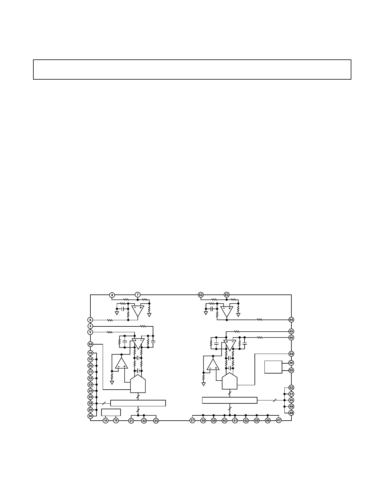
FUNCTIONAL BLOCK DIAGRAM
AMP-IN-A-2 AMP-IN-A-1
AMP-IN-B-2 AMP-IN-B-1
AMP-OUT-A
A–IN
A+IN
DROUTA
AMP-OUT-B
B+IN
B–IN
(LSB) D0A
D1A
D2A
D3A
D4A
D5A
D6A
D7A
D8A
D9A
D10A
AD13465
VREF
DROUT
14
11
100⍀ OUTPUT TERMINATORS
TIMING
3
VREF
DROUT
14
100⍀ OUTPUT TERMINATORS
9
TIMING
5
DROUTB
ENC
ENC
D13B (MSB)
D12B
D11B
D10B
D9B
REV. 0
ENC ENC D11A D12A D13A
(MSB)
D0B D1B D2B D3B D4B D5B D6B D7B D8B
(LSB)
Information furnished by Analog Devices is believed to be accurate and
reliable. However, no responsibility is assumed by Analog Devices for its
use, nor for any infringements of patents or other rights of third parties that
may result from its use. No license is granted by implication or otherwise
under any patent or patent rights of Analog Devices.
One Technology Way, P.O. Box 9106, Norwood, MA 02062-9106, U.S.A.
Tel: 781/329-4700
www.analog.com
Fax: 781/326-8703
© Analog Devices, Inc., 2001
1 page 
Pin No.
1, 35
2, 3, 9, 10, 13, 16
Mnemonic
SHIELD
AGNDA
4
5
6
7
8
11
12
14
15
17
18–25, 28–33
26, 27
34
36
37–42, 45–52
43, 44
53
54, 57, 60, 61, 67, 68
55
56
58
59
62
63
64
65
66
A–IN
A+IN
AMP-OUT-A
AMP-IN-A-1
AMP-IN-A-2
AVEEA
AVCCA
ENCA
ENCA
DVCCA
D0A–D13A
DGNDA
DROUTA
DROUTB
D0B–D13B
DGNDB
DVCCB
AGNDB
ENCB
ENCB
AVCCB
AVEEB
AMP-IN-B-2
AMP-IN-B-1
AMP-OUT-B
B+IN
B–IN
AD13465
PIN FUNCTION DESCRIPTIONS
Function
Internal Ground Shield Between Channels.
A Channel Analog Ground. A and B grounds should be connected as close to the
device as possible.
Inverting Differential Input (Gain = 1).
Noninverting Differential Input (Gain = 1).
Single-Ended Amplifier Output (Gain = 2).
Analog Input for A Side ADC (Nominally ± 0.5 V).
Analog Input for A Side ADC (Nominally ± 1.0 V).
A Channel Analog Negative Supply Voltage (Nominally –5.0 V or –5.2 V).
A Channel Analog Positive Supply Voltage (Nominally 5.0 V).
Complement of Encode; Differential Input.
Encode Input; Conversion Initiated on Rising Edge.
A Channel Digital Positive Supply Voltage (Nominally 5.0 V/3.3 V).
Digital Outputs for ADC A. D0 (LSB).
A Channel Digital Ground.
Data Ready A Output.
Data Ready B Output.
Digital Outputs for ADC B. D0 (LSB).
B Channel Digital Ground.
B Channel Digital Positive Supply Voltage (Nominally 5.0 V/3.3 V).
B Channel Analog Ground.
Encode Input; Conversion Initiated on Rising Edge.
Complement of Encode; Differential Input.
B Channel Analog Positive Supply Voltage (Nominally 5.0 V).
B Channel Analog Negative Supply Voltage (Nominally –5.0 V or –5.2 V).
Analog Input for B Side ADC (Nominally ± 1.0 V).
Analog Input for B Side ADC (Nominally ± 0.5 V).
Single-Ended Amplifier Output (Gain = 2).
Noninverting Differential Input (Gain = 1).
Inverting Differential Input (Gain = 1).
PIN CONFIGURATION
9 8 7 6 5 4 3 2 1 68 67 66 65 64 63 62 61
AGNDA 10
AVEEA 11
AVCCA 12
AGNDA 13
ENCA 14
ENCA 15
AGNDA 16
DVCCA 17
D0A(LSB) 18
D1A 19
D2A 20
D3A 21
D4A 22
D5A 23
D6A 24
D7A 25
DGNDA 26
PIN 1
IDENTIFIER
AD13465
TOP VIEW
(Not to Scale)
60 AGNDB
59 AVEEB
58 AVCCB
57 AGNDB
56 ENCB
55 ENCB
54 AGNDB
53 DVCCB
52 D13B(MSB)
51 D12B
50 D11B
49 D10B
48 D9B
47 D8B
46 D7B
45 D6B
44 DGNDB
27 28 29 30 31 32 33 34 35 36 37 38 39 40 41 42 43
REV. 0
–5–
5 Page 
AD13465
Power Supplies
Care should be taken when selecting a power source. Linear
supplies are strongly recommended. Switching supplies tend to
have radiated components that may be received by the AD13465.
Each of the power supply pins should be decoupled as closely to
the package as possible, using 0.1 µF chip capacitors.
The AD13465 has separate digital and analog power supply pins.
The analog supplies are denoted AVCC and the digital supply
pins are denoted DVCC. AVCC and DVCC should be separate
power supplies. This is because the fast digital output swings
can couple switching current back into the analog supplies.
Note that AVCC must be held within +5% and –3% of 5 V. The
AD13465 is specified for DVCC = 3.3 V as this is a common
supply for digital ASICs.
Output Loading
Care must be taken when designing the data receivers for the
AD13465. The digital outputs drive an internal series resistor
(e.g., 100 Ω) followed by a gate like 75LCX574. To minimize
capacitive loading, there should be only one gate on each output
pin. An example of this is shown in the evaluation board sche-
matic shown in Figure 10. The digital outputs of the AD13465
have a constant output slew rate of 1 V/ns. A typical CMOS
gate combined with a PCB trace will have a load of approximately
10 pF. Therefore, as each bit switches, 10 mA (10 pF × 1 V ÷ 1 ns)
of dynamic current per bit will flow in or out of the device. A full-
scale transition can cause up to 140 mA (14 bits × 10 mA/bit)
of transient current through the output stages. These switch-
ing currents are confined between ground and the DVCC pin.
Standard TTL gates should be avoided since they can apprecia-
bly add to the dynamic switching currents of the AD13465. It
should also be noted that extra capacitive loading will increase
output timing and invalidate timing specifications. Digital out-
put timing is guaranteed with 10 pF loads.
LAYOUT INFORMATION
The schematic of the evaluation board (Figure 10) represents a
typical implementation of the AD13465. The pinout of the
AD13465 is very straightforward and facilitates ease of use and
the implementation of high frequency/high resolution design
practices. It is recommended that high quality ceramic chip
capacitors be used to decouple each supply pin to ground directly
at the device. All capacitors can be standard high quality ceramic
chip capacitors.
Care should be taken when placing the digital output runs.
Because the digital outputs have such a high slew rate, the
capacitive loading on the digital outputs should be minimized.
Circuit traces for the digital outputs should be kept short and
connect directly to the receiving gate. Internal circuitry buffers
the outputs of the ADC through a resistor network to eliminate
the need to externally isolate the device from the receiving gate.
EVALUATION BOARD
The AD13465 evaluation board (Figure 9) is designed to
provide optimal performance for evaluation of the AD13465
analog-to-digital converter. The board encompasses everything
needed to ensure the highest level of performance for evaluating
the AD13465. The board requires an analog input signal, encode
clock, and power supply inputs. The clock is buffered on-board
to provide clocks for the latches. The digital outputs and out
clocks are available at the standard 40-pin connectors J1 and J2.
Power to the analog supply pins is connected via banana jacks.
The analog supply powers the associated components and
the analog section of the AD13465. The digital outputs of the
AD13465 are powered via banana jacks with 3.3 V. Contact the
factory if additional layout or applications assistance is required.
REV. 0
Figure 9. Evaluation Board Mechanical Layout
–11–
11 Page | ||
| Páginas | Total 20 Páginas | |
| PDF Descargar | [ Datasheet AD13465.PDF ] | |
Hoja de datos destacado
| Número de pieza | Descripción | Fabricantes |
| AD13465 | Dual Channel/ 14-Bit/ 65 MSPS A/D Converter with Analog Input Signal Conditioning | Analog Devices |
| Número de pieza | Descripción | Fabricantes |
| SLA6805M | High Voltage 3 phase Motor Driver IC. |
Sanken |
| SDC1742 | 12- and 14-Bit Hybrid Synchro / Resolver-to-Digital Converters. |
Analog Devices |
|
DataSheet.es es una pagina web que funciona como un repositorio de manuales o hoja de datos de muchos de los productos más populares, |
| DataSheet.es | 2020 | Privacy Policy | Contacto | Buscar |