|
|
|
PDF AD570 Data sheet ( Hoja de datos )
| Número de pieza | AD570 | |
| Descripción | Complete 8-Bit A-to-D Converter | |
| Fabricantes | Analog Devices | |
| Logotipo | ||
Hay una vista previa y un enlace de descarga de AD570 (archivo pdf) en la parte inferior de esta página. Total 8 Páginas | ||
|
No Preview Available !
a
FEATURES
Complete A/D Converter with Reference and Clock
Fast Successive Approximation Conversion: 25 s
No Missing Codes Over Temperature
0؇C to +70؇C: AD570J
–55؇C to +125؇C: AD570S
Digital Multiplexing: Three-State Outputs
18-Pin Ceramic DIP
Low Cost Monolithic Construction
Complete 8-Bit
A-to-D Converter
AD570*
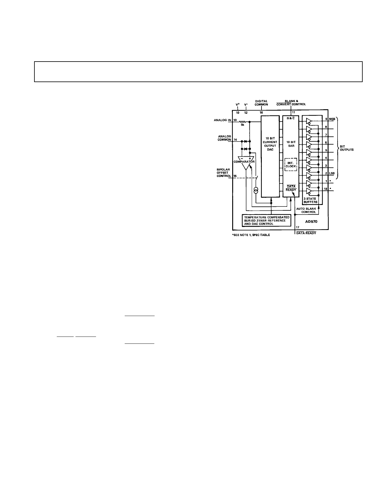
FUNCTIONAL BLOCK DIAGRAM
PRODUCT DESCRIPTION
The AD570 is an 8-bit successive approximation A/D converter
consisting of a DAC, voltage reference, clock, comparator, suc-
cessive approximation register and output buffers—all fabricated
on a single chip. No external components are required to per-
form a full accuracy 8-bit conversion in 25 µs.
The AD570 incorporates the most advanced integrated circuit
design and processing technology available today. I2L (inte-
grated injection logic) processing in the fabrication of the SAR
function along with laser trimming of the high stability SiCr
thin-film resistor ladder network at the wafer stage (LWT) and a
temperature compensated, subsurface Zener reference insures
full 8-bit accuracy at low cost.
Operating on supplies of +5 V and –15 V, the AD570 accepts
analog inputs of 0 V to +10 V unipolar of ± 5 V bipolar, exter-
nally selectable. As the BLANK and CONVERT input is driven
low, the three-state outputs go into the high impedance state
and a conversion commences. Upon completion of the conver-
sion, the DATA READY line goes low and the data appears at
the output. Pulling the BLANK and CONVERT input high
three states the outputs and readies the device for the next con-
version. The AD570 executes a true 8-bit conversion with no
missing codes in approximately 25 µs.
The AD570 is available in two version; the AD570J is specified
for the 0°C to +70°C temperature range, the AD570S for –55°C
to +125°C. Both guarantee full 8-bit accuracy and no missing
codes over their respective temperature ranges.
*U.S. Patents Numbered: 3,940,760; 4,213,806 and 4,136,349.
PRODUCT HIGHLIGHTS
1. The AD570 is a complete 8-bit A/D converter. No external
components are required to perform a conversion. Full-scale
calibration accuracy of ± 0.8% (2 LSB of 8 bits) is achieved
without external trims.
2. The AD570 is a single chip device employing the most ad-
vanced IC processing techniques. Thus, the user has at his
disposal a truly precision component with the reliability and
low cost inherent in monolithic construction,
3. The AD570 accepts either unipolar (0 V to +10 V) or bipolar
(–5 V to +5 V) analog inputs by grounding or opening a
single pin.
4. The device offers true 8-bit accuracy and exhibits no missing
codes over its entire operating temperature range.
5. Operation is guaranteed with –15 V and +5 V supplies. The
device will also operate with a –12 V supply.
6. The AD570S is also available processed to MIL-STD-883C,
Class B. The military data sheet for the AD570SD/883B is
included in the Analog Devices Military Products Databook.
REV. A
Information furnished by Analog Devices is believed to be accurate and
reliable. However, no responsibility is assumed by Analog Devices for its
use, nor for any infringements of patents or other rights of third parties
which may result from its use. No license is granted by implication or
otherwise under any patent or patent rights of Analog Devices.
One Technology Way, P.O. Box 9106, Norwood, MA 02062-9106, U.S.A.
Tel: 617/329-4700
Fax: 617/326-8703
1 page 
ZERO OFFSET
The apparent zero point of the AD570 can be adjusted by in-
serting an offset voltage between the analog common of the de-
vice and the actual signal return or signal common. Figure 7
illustrates two methods of providing this offset. Figure 7a shows
how the converter zero may be offset by up to ± 3 bits to correct
the device initial offset and/or input signal offsets. As shown, the
circuit gives approximately symmetrical adjustment in unipolar
mode. In bipolar mode R2 should be omitted to obtain a sym-
metrical range.
AD570
Figure 7a.
Figure 7b.
Figure 8 shows the nominal transfer curve near zero for an
AD570 in unipolar mode. The code transitions are at the edges
of the nominal bit weights. In some applications it will be pref-
erable to offset the code transitions so that they fall between the
nominal bit weights, as shown in the offset characteristics. This
offset can easily be accomplished as shown in Figure 7b.
At balance (after a conversion) approximately 2 mA flows into
the analog common terminal. A 10 Ω resistor in series with this
terminal will result in approximately the desired 1/2 bit offset of
the transfer characteristics. The nominal 2 mA analog common
current is not closely controlled in manufacture. If high accuracy
is required, a 20 Ω potentiometer (connected as a rheostat) can
be used as R1. Additional negative offset range may be obtained
by using larger values of R1. Of course, if the zero transition
point is changed, the full-scale transition point will also move.
Thus, if an offset of 1/2 LSB is introduced, full-scale trimming
as described on previous page should be done with an analog
input of 9.941 volts.
Figure 8. AD570 Transfer Curve—Unipolar Operation
(Approximate Bit Weights Shown for Illustration, Nominal
Bit Weights ϳ 36.1 mV)
NOTE: During a conversion transient currents from the analog
common terminal will disturb the offset voltage. Capacitive de-
coupling should not be used around the offset network. These
transients will settle as appropriate during a conversion. Capaci-
tive decoupling will “pump up” and fail to settle resulting in
conversion errors. Power supply decoupling which returns to
analog signal common should go to the signal input side of the
resistive offset network.
CONTROL AND TIMING OF THE AD570
There are several important timing and control features on the
AD570 which must be understood precisely to allow optimal
interfacing to microprocessor or other types of control systems.
All of these features are shown in the timing diagram in Figure 9.
The normal standby situation is shown at the left end of the
drawing. The BLANK and CONVERT (B & C) line is held
high, the output lines will be “open”, and the DATA READY
(DR) line will be high. This mode is the lowest power state of
the device (typically 150 mW). When the (B & C ) line is
brought low, the conversion cycle is initiated; but the DR and
data lines do not change state. When the conversion cycle is
complete (typically 25 µs), the DR line goes low, and within
500 ns, the data lines become active with the new data.
About 1.5 µs after the B & C line is again brought high, the DR
line will go high and the data lines will go open. When the
B & C line is again brought low, a new conversion will begin.
The minimum pulse width for the B & C line to blank previous
data and start a new conversion is 2 µs. If the B & C line is
brought high during a conversion, the conversion will stop, and
REV. A
–5–
5 Page | ||
| Páginas | Total 8 Páginas | |
| PDF Descargar | [ Datasheet AD570.PDF ] | |
Hoja de datos destacado
| Número de pieza | Descripción | Fabricantes |
| AD570 | Complete 8-Bit A-to-D Converter | Analog Devices |
| AD5700 | Low Power HART Modem | Analog Devices |
| AD5700-1 | Low Power HART Modem | Analog Devices |
| AD571 | 10-Bit A/D Converter | Analog Devices |
| Número de pieza | Descripción | Fabricantes |
| SLA6805M | High Voltage 3 phase Motor Driver IC. |
Sanken |
| SDC1742 | 12- and 14-Bit Hybrid Synchro / Resolver-to-Digital Converters. |
Analog Devices |
|
DataSheet.es es una pagina web que funciona como un repositorio de manuales o hoja de datos de muchos de los productos más populares, |
| DataSheet.es | 2020 | Privacy Policy | Contacto | Buscar |