|
|
|
PDF AD546 Data sheet ( Hoja de datos )
| Número de pieza | AD546 | |
| Descripción | 1 pA Monolithic Electrometer Operational Amplifier | |
| Fabricantes | Analog Devices | |
| Logotipo | ||
Hay una vista previa y un enlace de descarga de AD546 (archivo pdf) en la parte inferior de esta página. Total 12 Páginas | ||
|
No Preview Available !
a
FEATURES
DC PERFORMANCE
1 mV max Input Offset Voltage
Low Offset Drift: 20 V/؇C
1 pA max Input Bias Current
Input Bias Current Guaranteed Over Full
Common-Mode Voltage Range
AC PERFORMANCE
3 V/s Slew Rate
1 MHz Unity Gain Bandwidth
Low Input Voltage Noise: 4 V p-p, 0.1 Hz to 10 Hz
Available in a Low Cost, 8-Pin Plastic Mini-DIP
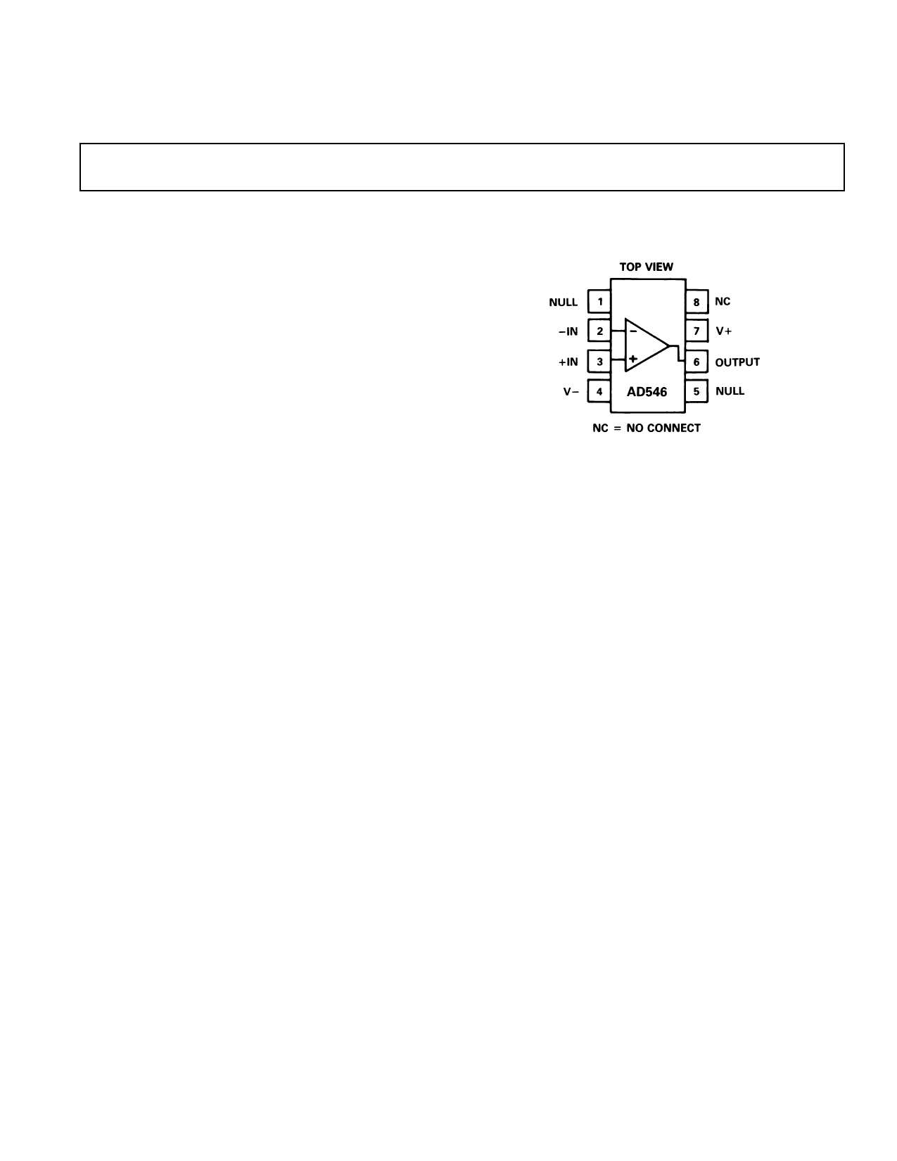
Standard Op Amp Pinout
APPLICATIONS
Electrometer Amplifiers
Photodiode Preamps
pH Electrode Buffers
Log Ratio Amplifiers
1 pA Monolithic Electrometer
Operational Amplifier
AD546*
CONNECTION DIAGRAM
8-Pin Plastic
Mini-DIP Package
PRODUCT DESCRIPTION
The AD546 is a monolithic electrometer combining the virtues
of low (1 pA) input bias current with the cost effectiveness of a
plastic mini-DIP package. Both input offset voltage and input
offset voltage drift are laser trimmed, providing very high perfor-
mance for such a low cost amplifier.
Input bias currents are reduced significantly by using “topgate”
JFET technology. The 1015 Ω common-mode impedance,
resulting from a bootstrapped input stage, insures that input
bias current is essentially independent of common-mode voltage
variations.
The AD546 is suitable for applications requiring both minimal
levels of input bias current and low input offset voltage. Appli-
cations for the AD546 include use as a buffer amplifier for cur-
rent output transducers such as photodiodes and pH probes. It
may also be used as a precision integrator or as a low droop rate
sample and hold amplifier. The AD546 is pin compatible with
standard op amps; its plastic mini-DIP package is ideal for use
with automatic insertion equipment.
The AD546 is available in two performance grades, all rated
over the 0°C to +70°C commercial temperature range, and
packaged in an 8-pin plastic mini-DIP.
PRODUCT HIGHLIGHTS
1. The input bias current of the AD546 is specified, 100%
tested and guaranteed with the device in the fully warmed-up
condition.
2. The input offset voltage of the AD546 is laser trimmed to
less than 1 mV (AD546K).
3. The AD546 is packaged in a standard, low cost, 8-pin
mini-DIP.
4. A low quiescent supply current of 700 µA minimizes any
thermal effects which might degrade input bias current and
input offset voltage specifications.
*Covered by Patent No. 4,639,683.
REV. A
Information furnished by Analog Devices is believed to be accurate and
reliable. However, no responsibility is assumed by Analog Devices for its
use, nor for any infringements of patents or other rights of third parties
which may result from its use. No license is granted by implication or
otherwise under any patent or patent rights of Analog Devices.
One Technology Way, P.O. Box 9106, Norwood, MA 02062-9106, U.S.A.
Tel: 617/329-4700
Fax: 617/326-8703
1 page 
300
250
200
150
+25oC
100
0
5 10 15
SUPPLY VOLTAGE ± VOLTS
20
Figure 10. Input Bias Current
vs. Supply Voltage
160
140
120
100
80
60
40
20
10
100
1k 10k
FREQUENCY – Hz
Figure 11. Input Voltage Noise
Spectral Density vs. Frequency
AD546
100k WHENEVER JOHNSON NOISE IS GREATER THAN
AMPLIFIER NOISE, AMPLIFIER NOISE CAN BE
CONSIDERED NEGLIGIBLE FOR THE APPLICATION.
10k
1 kHz BANDWIDTH
1k
RESISTOR JOHNSON NOISE
100
10
10 Hz
BANDWIDTH
1
0.1
100k
AMPLIFIER GENERATED NOISE
1M 10M 100M 1G 10G
SOURCE RESISTANCE – Ohms
100G
Figure 12. Noise vs. Source
Resistance
100 100
80 80
60 60
40 40
20 20
00
–20 –20
–40
10 100 1k
–40
10k 100k 1M 10M
FREQUENCY – Hz
Figure 13. Open Loop Frequency
Response
40
35
30
25
20
15
10
5
0
10 100 1k 10k 100k 1M
FREQUENCY – Hz
Figure 14. Large Signal Frequency
Response
Figure 15. CMRR vs. Frequency
Figure 16. PSRR vs. Frequency
Figure 17. Output Settling Time vs.
Output Swing and Error Voltage
REV. A
–5–
5 Page 
AD546
tacting the device under test. Rigid Teflon coaxial cable is used
to make connections to all high impedance nodes. The use of
rigid coax affords immunity to error induced by mechanical vi-
bration and provides an outer conductor for shielding. The en-
tire circuit is enclosed in a grounded metal box.
The test apparatus is calibrated without a device under test
present. A five minute stabilization period after the power is
turned on is required. First, VERR1 and VERR2 are measured.
These voltages are the errors caused by offset voltages and leak-
age currents of the current to voltage converters.
VERR1 = 10 (VOSA – IBA × RSa)
VERR2 = 10 (VOSB – IBB × RSb)
Once measured, these errors are subtracted from the readings
taken with a device under test present. Amplifier B closes the
feedback loop to the device under test, in addition to providing
current to voltage conversion. The offset error of the device un-
der test appears as a common-mode signal and does not affect
the test measurement. As a result, only the leakage current of
the device under test is measured.
VA – VERR1 = 10[RSa × IB(+)]
VX – VERR2 = 10[RSb × IB(–)]
Although a series of devices can be tested after only one calibra-
tion measurement, calibration should be updated periodically to
compensate for any thermal drift of the current-to-voltage con-
verters or changes in the ambient environment. Laboratory re-
sults have shown that repeatable measurements within 10 fA can
be realized when this apparatus is properly implemented. These
results are achieved in part by the design of the circuit, which
eliminates relays and other parasitic leakage paths in the high
impedance signal lines, and in part by the inherent cancellation
of errors through the calibration and measurement procedure.
PHOTODIODE INTERFACE
The AD546’s 1 pA current and low input offset voltage make it
a good choice for very sensitive photodiode preamps (Figure
39). The photodiode develops a signal current, IS, equal to:
IS = R × P
where P is light power incident on the diode’s surface in watts
and R is the photodiode responsivity in amps/watt. RF converts
the signal current to an output voltage:
VOUT = RF × IS
Input current, IB, will contribute an output voltage error, VE1,
proportional to the feedback resistance:
VE1 = IB × RF
The op amp’s input voltage offset will cause an error current
through the photodiode’s shunt resistance, RS:
I = VOS/RS
The error current will result in an error voltage (VE2) at the
amplifier’s output equal to:
VE2 = (1 +RF/RS) VOS
Given typical values of photodiode shunt resistance (on the or-
der of 109 Ω), RF/RS can be greater than one, especially if a large
feedback resistance is used. Also, RF/RS will increase with tem-
perature, as photodiode shunt resistance typically drops by a
factor of two for every 10°C rise in temperature. An op amp
with low offset voltage and low drift helps maintain accuracy.
Figure 40. Photodiode Preamp DC Error Sources
Photodiode Preamp Noise
Noise limits the signal resolution obtainable with the preamp.
The output voltage noise divided by the feedback resistance is
the minimum current signal that can be detected. This mini-
mum detectable current divided by the responsivity of the pho-
todiode represents the lowest light power that can be detected
by the preamp.
Noise sources associated with the photodiode, amplifier, and
feedback resistance are shown in Figure 41; Figure 42 is the
voltage spectral density versus frequency plot of each of the
noise source’s contribution to the output voltage noise (circuit
parameters in Figure 40 are assumed). Each noise source’s rms
contribution to the total output voltage noise is obtained by in-
tegrating the square of its spectral density function over fre-
quency. The rms value of the output voltage noise is the square
root of the sum of all contributions. Minimizing the total area
under these curves will optimize the preamplifier’s resolution for
a given bandwidth.
Figure 39. Photodiode Preamp
DC error sources and an equivalent circuit for a small area
(0.2 mm square) photodiode are indicated in Figure 40.
REV. A
–11–
Figure 41. Photodiode Preamp Noise Sources
11 Page | ||
| Páginas | Total 12 Páginas | |
| PDF Descargar | [ Datasheet AD546.PDF ] | |
Hoja de datos destacado
| Número de pieza | Descripción | Fabricantes |
| AD5405 | Dual 12-Bit/ High Bandwidth/ Multiplying DAC with 4-Quadrant Resistors and Parallel Interface | Analog Devices |
| AD5410 | Current Source DAC | Analog Devices |
| AD5412 | (AD5412 / AD5422) Current Source & Voltage Output DAC | Analog Devices |
| AD5415 | (AD5424 - AD5547) High Bandwidth Multiplying DACs | Analog Devices |
| Número de pieza | Descripción | Fabricantes |
| SLA6805M | High Voltage 3 phase Motor Driver IC. |
Sanken |
| SDC1742 | 12- and 14-Bit Hybrid Synchro / Resolver-to-Digital Converters. |
Analog Devices |
|
DataSheet.es es una pagina web que funciona como un repositorio de manuales o hoja de datos de muchos de los productos más populares, |
| DataSheet.es | 2020 | Privacy Policy | Contacto | Buscar |