|
|
|
PDF AD536 Data sheet ( Hoja de datos )
| Número de pieza | AD536 | |
| Descripción | Integrated Circuit True RMS-to-DC Converter | |
| Fabricantes | Analog Devices | |
| Logotipo | ||
Hay una vista previa y un enlace de descarga de AD536 (archivo pdf) en la parte inferior de esta página. Total 8 Páginas | ||
|
No Preview Available !
a
Integrated Circuit
True RMS-to-DC Converter
AD536A
FEATURES
True RMS-to-DC Conversion
Laser-Trimmed to High Accuracy
0.2% Max Error (AD536AK)
0.5% Max Error (AD536AJ)
Wide Response Capability:
Computes RMS of AC and DC Signals
450 kHz Bandwidth: V rms > 100 mV
2 MHz Bandwidth: V rms > 1 V
Signal Crest Factor of 7 for 1% Error
dB Output with 60 dB Range
Low Power: 1.2 mA Quiescent Current
Single or Dual Supply Operation
Monolithic Integrated Circuit
–55؇C to +125؇C Operation (AD536AS)
PRODUCT DESCRIPTION
The AD536A is a complete monolithic integrated circuit which
performs true rms-to-dc conversion. It offers performance which
is comparable or superior to that of hybrid or modular units
costing much more. The AD536A directly computes the true
rms value of any complex input waveform containing ac and dc
components. It has a crest factor compensation scheme which
allows measurements with 1% error at crest factors up to 7. The
wide bandwidth of the device extends the measurement capabi-
lity to 300 kHz with 3 dB error for signal levels above 100 mV.
An important feature of the AD536A not previously available in
rms converters is an auxiliary dB output. The logarithm of the
rms output signal is brought out to a separate pin to allow the
dB conversion, with a useful dynamic range of 60 dB. Using an
externally supplied reference current, the 0 dB level can be con-
veniently set by the user to correspond to any input level from
0.1 to 2 volts rms.
The AD536A is laser trimmed at the wafer level for input and
output offset, positive and negative waveform symmetry (dc re-
versal error), and full-scale accuracy at 7 V rms. As a result, no
external trims are required to achieve the rated unit accuracy.
There is full protection for both inputs and outputs. The input
circuitry can take overload voltages well beyond the supply lev-
els. Loss of supply voltage with inputs connected will not cause
unit failure. The output is short-circuit protected.
The AD536A is available in two accuracy grades (J, K) for com-
mercial temperature range (0°C to +70°C) applications, and one
grade (S) rated for the –55°C to +125°C extended range. The
AD536AK offers a maximum total error of ± 2 mV ± 0.2% of
reading, and the AD536AJ and AD536AS have maximum errors
of ± 5 mV ± 0.5% of reading. All three versions are available in
either a hermetically sealed 14-lead DIP or 10-pin TO-100
metal can. The AD536AS is also available in a 20-leadless her-
metically sealed ceramic chip carrier.
REV. B
Information furnished by Analog Devices is believed to be accurate and
reliable. However, no responsibility is assumed by Analog Devices for its
use, nor for any infringements of patents or other rights of third parties
which may result from its use. No license is granted by implication or
otherwise under any patent or patent rights of Analog Devices.
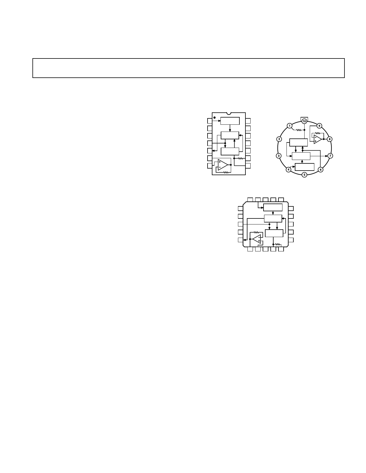
PIN CONFIGURATIONS AND
FUNCTIONAL BLOCK DIAGRAMS
TO-116 (D-14) and
Q-14 Package
TO-100 (H-10A)
Package
VIN 1
ABSOLUTE
VALUE
NC 2 AD536A
–VS 3
SQUARER
DIVIDER
CAV 4
14 +VS
13 NC
12 NC
11 NC
IOUT
COM
RL 25k⍀
AD536A
CURRENT
MIRROR
BUF IN
25k⍀
BUF
OUT
BUF
dB 5
BUF
OUT
6
BUF
IN
7
CURRENT
MIRROR
10 COM
BUF
25k⍀
25k⍀ 9 RL
8 IOUT
+VS
VIN
SQUARER
DIVIDER
ABSOLUTE
VALUE
NC = NO CONNECT
–VS
LCC (E-20A) Package
dB
CAV
NC VIN NC +VS NC
3 2 1 20 19
–VS 4
NC 5
CAV 6
NC 7
dB 8
AD536A
ABSOLUTE
VALUE
SQUARER
DIVIDER
25k⍀
CURRENT
MIRROR
BUF
25k⍀
9 10 11 12 13
BUF BUF NC IOUT RL
OUT IN
NC = NO CONNECT
18 NC
17 NC
16 NC
15 NC
14 COM
PRODUCT HIGHLIGHTS
1. The AD536A computes the true root-mean-square level of a
complex ac (or ac plus dc) input signal and gives an equiva-
lent dc output level. The true rms value of a waveform is a
more useful quantity than the average rectified value since it
relates directly to the power of the signal. The rms value of a
statistical signal also relates to its standard deviation.
2. The crest factor of a waveform is the ratio of the peak signal
swing to the rms value. The crest factor compensation
scheme of the AD536A allows measurement of highly com-
plex signals with wide dynamic range.
3. The only external component required to perform measure-
ments to the fully specified accuracy is the capacitor which
sets the averaging period. The value of this capacitor determines
the low frequency ac accuracy, ripple level and settling time.
4. The AD536A will operate equally well from split supplies or
a single supply with total supply levels from 5 to 36 volts.
The one milliampere quiescent supply current makes the
device well-suited for a wide variety of remote controllers and
battery powered instruments.
5. The AD536A directly replaces the AD536 and provides im-
proved bandwidth and temperature drift specifications.
One Technology Way, P.O. Box 9106, Norwood, MA 02062-9106, U.S.A.
Tel: 781/329-4700 World Wide Web Site: http://www.analog.com
Fax: 781/326-8703
© Analog Devices, Inc., 1999
1 page 
factors, (such as low duty cycle pulse trains), the averaging time
constant should be at least ten times the signal period. For
example, a 100 Hz pulse rate requires a 100 ms time constant,
which corresponds to a 4 µF capacitor (time constant = 25 ms
per µF).
The primary disadvantage in using a large CAV to remove ripple
is that the settling time for a step change in input level is in-
creased proportionately. Figure 5 shows that the relationship
between CAV and 1% settling time is 115 milliseconds for each
microfarad of CAV. The settling time is twice as great for de-
creasing signals as for increasing signals (the values in Figure 5
are for decreasing signals). Settling time also increases for low
signal levels, as shown in Figure 6.
AD536A
The two-pole post-filter uses an active filter stage to provide
even greater ripple reduction without substantially increasing
the settling times over a circuit with a one-pole filter. The values
of CAV, C2, and C3 can then be reduced to allow extremely fast
settling times for a constant amount of ripple. Caution should
be exercised in choosing the value of CAV, since the dc error is
dependent upon this value and is independent of the post filter.
For a more detailed explanation of these topics refer to the
RMS to DC Conversion Application Guide 2nd Edition, available
from Analog Devices.
Figure 5. Error/Settling Time Graph for Use with the Stan-
dard rms Connection in Figure 1
C3
C2
C3
Figure 7. 2-Pole “Post” Filter
Figure 6. Settling Time vs. Input Level
A better method for reducing output ripple is the use of a
“post-filter.” Figure 7 shows a suggested circuit. If a single-pole
filter is used (C3 removed, RX shorted), and C2 is approximately
twice the value of CAV, the ripple is reduced as shown in Figure
8 and settling time is increased. For example, with CAV = 1 µF
and C2 = 2.2 µF, the ripple for a 60 Hz input is reduced from
10% of reading to approximately 0.3% of reading. The settling
time, however, is increased by approximately a factor of 3. The
values of CAV and C2, can, therefore, be reduced to permit faster
settling times while still providing substantial ripple reduction.
Figure 8. Performance Features of Various Filter Types
AD536A PRINCIPLE OF OPERATION
The AD536A embodies an implicit solution of the rms equation
that overcomes the dynamic range as well as other limitations
inherent in a straightforward computation of rms. The actual
computation performed by the AD536A follows the equation:
V
rms
=
Avg .
V IN 2
V rms
REV. B
–5–
5 Page | ||
| Páginas | Total 8 Páginas | |
| PDF Descargar | [ Datasheet AD536.PDF ] | |
Hoja de datos destacado
| Número de pieza | Descripción | Fabricantes |
| AD530 | Integrated Circuit / Multiplier / Divider / Square Rooter | Analog Devices |
| AD5300 | 8-Bit DAC | Analog Devices |
| AD5301 | +2.5 V to +5.5 V/ 120 uA/ 2-Wire Interface/ Voltage Output 8-/10-/12-Bit DACs | Analog Devices |
| AD5302 | +2.5 V to +5.5 V/ 230 uA Dual Rail-to-Rail/ Voltage Output 8-/10-/12-Bit DACs | Analog Devices |
| Número de pieza | Descripción | Fabricantes |
| SLA6805M | High Voltage 3 phase Motor Driver IC. |
Sanken |
| SDC1742 | 12- and 14-Bit Hybrid Synchro / Resolver-to-Digital Converters. |
Analog Devices |
|
DataSheet.es es una pagina web que funciona como un repositorio de manuales o hoja de datos de muchos de los productos más populares, |
| DataSheet.es | 2020 | Privacy Policy | Contacto | Buscar |