|
|
|
PDF AD7750 Data sheet ( Hoja de datos )
| Número de pieza | AD7750 | |
| Descripción | Product-to-Frequency Converter | |
| Fabricantes | Analog Devices | |
| Logotipo | ||
Hay una vista previa y un enlace de descarga de AD7750 (archivo pdf) en la parte inferior de esta página. Total 16 Páginas | ||
|
No Preview Available !
a
FEATURES
Two Differential Analog Input Channels
Product of Two Channels
Voltage-to-Frequency Conversion on a Single Channel
Real Power Measurement Capability
< 0.2% Error Over the Range 400% Ibasic to 2% Ibasic
Two or Four Quadrant Operation (Positive and
Negative Power)
Gain Select of 1 or 16 on the Current Channel (Channel 1)
Choice of On-Chip or External Reference
Choice of Output Pulse Frequencies Available
(Pins F1 and F2)
High Frequency Pulse Output for Calibration Purposes
(FOUT)
HPF on Current Channel for Offset Removal
Single 5 V Supply and Low Power
Product-to-Frequency
Converter
AD7750
FUNCTIONAL BLOCK DIAGRAM
G1 VDD ACDC
ADC1
REVP
V1+ 2ND ORDER
V1– x16 MODULATOR
DELAY
CLKOUT
HPF
CLKIN
ADC2
V2+ 2ND ORDER
V2– x2 MODULATOR
MULT
2.5V
BAND GAP
REFERENCE
LPF
AD7750
DTF
DTF
F1
F2
FOUT
AGND REFOUT
REFIN
FS S1 S2 DGND
GENERAL DESCRIPTION
The AD7750 is a Product-to-Frequency Converter (PFC)
that can be configured for power measurement or voltage-to-
frequency conversion. The part contains the equivalent of two
channels of A/D conversion, a multiplier, a digital-to-frequency
converter, a reference and other conditioning circuitry. Channel 1
has a differential gain amplifier with selectable gains of 1 or 16.
Channel 2 has a differential gain amplifier with a gain of 2. A high-
pass filter can be switched into the signal path of Channel 1 to
remove any offsets.
The outputs F1 and F2 are fixed width (275 ms) logic low going
pulse streams for output frequencies less than 1.8 Hz. A range
of output frequencies is available and the frequency of F1 and
F2 is proportional to the product of V1 and V2. These outputs
are suitable for directly driving an electromechanical pulse
counter or full stepping two phase stepper motors. The outputs
can be configured to represent the result of four-quadrant multi-
plication (i.e., Sign and Magnitude) or to represent the result of
a two quadrant multiplication (i.e., Magnitude Only). In this
configuration the outputs are always positive regardless of the
input polarities. In addition, there is a reverse polarity indicator
output that becomes active when negative power is detected in
the Magnitude Only Mode, see Reverse Polarity Indicator.
The error as a percent (%) of reading is less than 0.3% over a
dynamic range of 1000:1.
The AD7750 is fabricated on 0.6 µ CMOS technology; a pro-
cess that combines low power and low cost.
PRODUCT HIGHLIGHTS
1. The part can be configured for power measurement or
voltage-to-frequency conversion.
2. The output format and maximum frequency is selectable;
from low-frequency outputs, suitable for driving stepper
motors, to higher frequency outputs, suitable for calibration
and test.
3. There is a reverse polarity indicator output that becomes
active when negative power is detected in the Magnitude
Only Mode.
4. Error as a % of reading over a dynamic range of 1000:1 is
< 0.3%.
REV. 0
Information furnished by Analog Devices is believed to be accurate and
reliable. However, no responsibility is assumed by Analog Devices for its
use, nor for any infringements of patents or other rights of third parties
which may result from its use. No license is granted by implication or
otherwise under any patent or patent rights of Analog Devices.
One Technology Way, P.O. Box 9106, Norwood, MA 02062-9106, U.S.A.
Tel: 781/329-4700 World Wide Web Site: http://www.analog.com
Fax: 781/326-8703
© Analog Devices, Inc., 1997
1 page 
PIN CONFIGURATION
SOIC and DIP
VDD 1
G1 2
20 F1
19 F2
V1+ 3
18 FOUT
V1– 4
17 REVP
AGND 5 AD7750 16 CLKOUT
V2+
6
TOP VIEW
(Not to Scale)
15
CLKIN
V2– 7
14 ACDC
REFOUT 8
13 S1
REFIN 9
12 S2
DGND 10
11 FS
AD7750
Typical Performance Characteristics
140
120
AS PER DATA SHEET
100 CONDITIONS WITH
GAIN = 1
80
60
40
20
0
0 0.1 0.2 0.3 0.4 0.5 0.6 0.7 0.8
50Hz RIPPLE – V rms
Figure 1. PSR as a Function of VDD 50 Hz Ripple
0.6
0.4
0.2
0
–0.2
–0.4
–0.6
–0.8
45 46 47 48 49 50 51 52 53 54 55
LINE FREQUENCY – Hz
Figure 2. Phase Error as a Function of Line Frequency
120
AS PER DATA SHEET
100 CONDITIONS WITH
GAIN = 16
80
60
40
20
0
0 0.01
0.02 0.03 0.04 0.05 0.06 0.07 0.08 0.09
50Hz RIPPLE – V rms
Figure 3. PSR as a Function of VDD 50 Hz Ripple
REV. 0
–5–
5 Page 
AD7750
Table II. Maximum Output Frequencies
Mode
0
1
2
3
4
5
6
7
F1, F2 (Hz) FOUT (Hz)
FS S2 S1 (DC)
(DC)
0 0 0 6.8 ± 2.9
109 ± 46
0 0 1 0 to 2.9
0 to 23
0 1 0 0 to 2.9
0 to 46
0 1 1 6.8 ± 2.9
218 ± 142
1 0 0 13.6 ± 5.8 218 ± 92
1 0 1 0 to 5.8
0 to 92
1 1 0 0 to 5.8
0 to 184
1 1 1 13.6 ± 5.8 218 ± 142
F1, F2 (Hz)
(AC)
6.8 ± 1.45
0 to 1.45
0 to 1.45
6.8 ± 1.45
13.6 ± 2.9
0 to 2.9
0 to 2.9
13.6 ± 2.9
FOUT (Hz)
(AC)
109 ± 23
0 to 11.5
0 to 23
218 ± 142
218 ± 46
0 to 46
0 to 92
218 ± 142
ACDC
G1
TIME DELAY 143s
(CLKIN = 3.5795MHz)
HPF
2.58؇C AT 50Hz
V1+
PGA
ADC 1
V1–
τ
DIGITAL-TO-FREQUENCY BLOCK
COUNTER/ACCUMULATOR
CLKIN
LPF
FOUT
PHASE LEAD OF
2.58؇C AT 50Hz
DTF
F1
DIGITAL
MULTIPLIER
F2
V2+
X2 ADC 2
V2–
FS S2 S1
Figure 15. Equivalent AD7750 Signal Processing Chain
sRC
H(s) =
1 + sRC
C R R = 1M⍀
C = 0.0707F
Figure 16. HPF in Channel 1
R1
1M⍀
VR1
100⍀
R3
1.1k⍀
860:1 ATTENUTATION
C1
47nF
R2
33k⍀
VR2
200⍀
C2
33nF
R4
1.1k⍀
C3
33F
PIN 7
PIN 6
Figure 17. Phase Lag Compensation on Channel 1 for
60 Hz Line Frequency
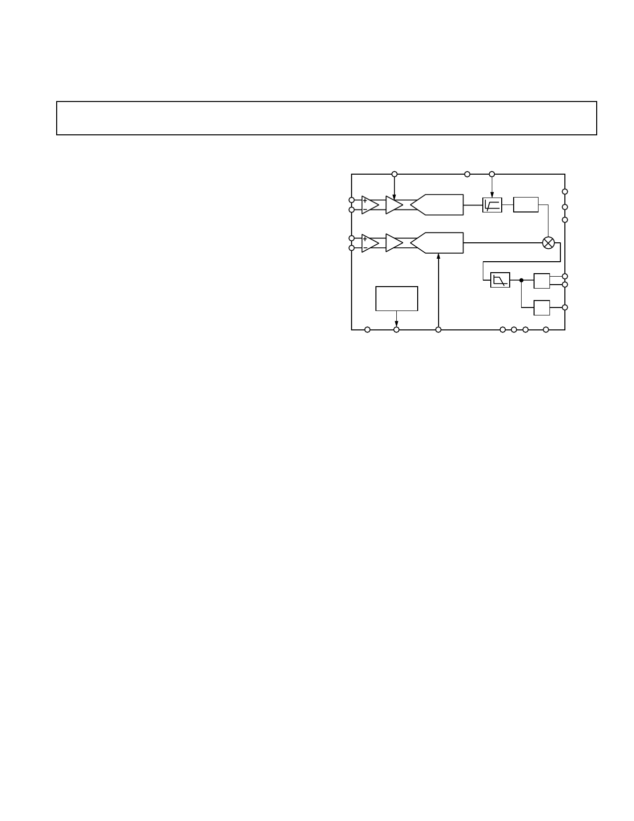
Digital-to-Frequency Converter (DTF)
After they have been filtered, the outputs of the two sigma-delta
modulators are fed into a digital multiplier. The output of the
multiplier is then low-pass filtered to obtain the real power
information. The output of the LPF enters a digital-to-frequency
converter whose output frequency is now proportional to the
real power. The DTF offers a range of output frequencies to
suit most power measurement applications. There is also a high
frequency output called FOUT, which can be used for calibra-
tion purposes. The output frequencies are determined by the
logic inputs FS, S2 and S1. This is explained in the section of
this data sheet called Determining the Output Frequencies of
the AD7750.
Figure 18 shows the waveforms of the various frequency out-
puts. The outputs F1 and F2 are the low frequency outputs
that can be used to directly drive a stepper motor or electrome-
chanical pulse counter. The F1 and F2 outputs provide two
alternating low going pulses. The pulsewidth is set at 275 ms
and the time between the falling edges of F1 and F2 is ap-
proximately half the period of F1. If, however, the period of
F1 and F2 falls below 550 ms (1.81 Hz) the pulsewidth of F1
and F2 is set to half the period. For example in Mode 3,
where F1 and F2 vary around 6.8 Hz, the pulsewidth would vary
from 1/2.(6.8+1.45) seconds to 1/2.(6.8–1.45) seconds—see
Table II.
REV. 0
–11–
11 Page | ||
| Páginas | Total 16 Páginas | |
| PDF Descargar | [ Datasheet AD7750.PDF ] | |
Hoja de datos destacado
| Número de pieza | Descripción | Fabricantes |
| AD775 | 8-Bit 20 MSPS/ 60 mW Sampling A/D Converter | Analog Devices |
| AD7750 | Product-to-Frequency Converter | Analog Devices |
| AD7751 | Energy Metering IC With On-Chip Fault Detection | Analog Devices |
| AD7755 | Energy Metering IC with Pulse Output | Analog Devices |
| Número de pieza | Descripción | Fabricantes |
| SLA6805M | High Voltage 3 phase Motor Driver IC. |
Sanken |
| SDC1742 | 12- and 14-Bit Hybrid Synchro / Resolver-to-Digital Converters. |
Analog Devices |
|
DataSheet.es es una pagina web que funciona como un repositorio de manuales o hoja de datos de muchos de los productos más populares, |
| DataSheet.es | 2020 | Privacy Policy | Contacto | Buscar |