|
|
|
PDF AD7710 Data sheet ( Hoja de datos )
| Número de pieza | AD7710 | |
| Descripción | Signal Conditioning ADC | |
| Fabricantes | Analog Devices | |
| Logotipo | ||
Hay una vista previa y un enlace de descarga de AD7710 (archivo pdf) en la parte inferior de esta página. Total 28 Páginas | ||
|
No Preview Available !
a
Signal Conditioning ADC
AD7710*
FEATURES
Charge Balancing ADC
24 Bits No Missing Codes
؎0.0015% Nonlinearity
Two-Channel Programmable Gain Front End
Gains from 1 to 128
Differential Inputs
Low-Pass Filter with Programmable Filter Cutoffs
Ability to Read/Write Calibration Coefficients
Bidirectional Microcontroller Serial Interface
Internal/External Reference Option
Single or Dual Supply Operation
Low Power (25 mW typ) with Power-Down Mode
(7 mW typ)
APPLICATIONS
Weigh Scales
Thermocouples
Process Control
Smart Transmitters
Chromatography
GENERAL DESCRIPTION
The AD7710 is a complete analog front end for low frequency
measurement applications. The device accepts low level signals
directly from a strain gage or transducer and outputs a serial
digital word. It employs a sigma-delta conversion technique to
realize up to 24 bits of no missing codes performance. The input
signal is applied to a proprietary programmable gain front end
based around an analog modulator. The modulator output is
processed by an on-chip digital filter. The first notch of this
digital filter can be programmed via the on-chip control register
allowing adjustment of the filter cutoff and settling time.
The part features two differential analog inputs and a differen-
tial reference input. Normally, one of the channels will be used
as the main channel with the second channel used as an auxil-
iary input to periodically measure a second voltage. It can be
operated from a single supply (by tying the VSS pin to AGND)
provided that the input signals on the analog inputs are more
positive than –30 mV. By taking the VSS pin negative, the part
can convert signals down to –VREF on its inputs. The AD7710
thus performs all signal conditioning and conversion for a single
or dual channel system.
The AD7710 is ideal for use in smart, microcontroller based
systems. Input channel selection, gain settings and signal polar-
ity can be configured in software using the bidirectional serial
port. The AD7710 contains self-calibration, system calibration
and background calibration options and also allows the user to
read and write the on-chip calibration registers.
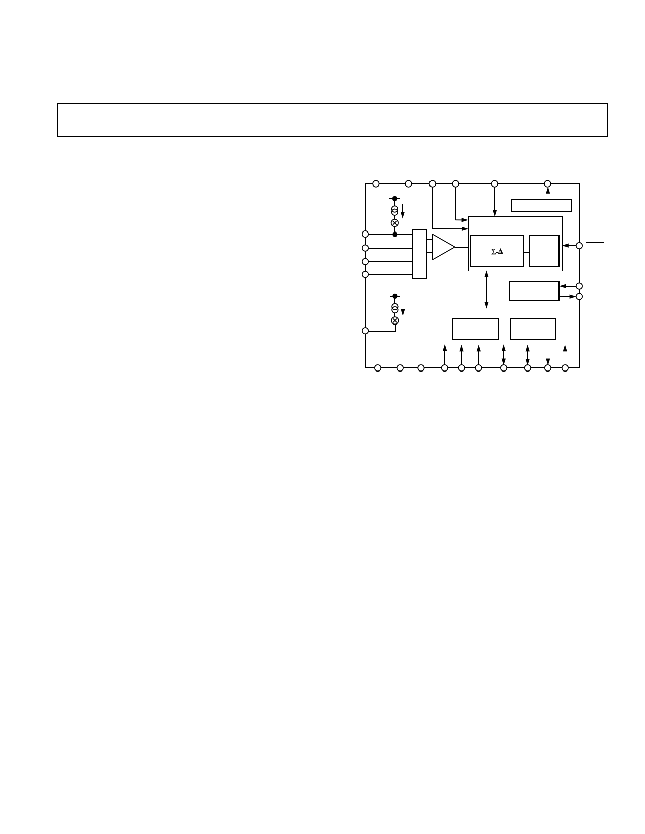
FUNCTIONAL BLOCK DIAGRAM
AVDD
REF REF
DVDD IN (–) IN (+)
AVDD
VBIAS
REF OUT
AIN1(+)
AIN1(–)
AIN2(+)
AIN2(–)
4.5A
M PGA
U
X
A = 1 – 128
2.5V REFERENCE
CHARGE-BALANCING A/D
CONVERTER
AUTO-ZEROED
MODULATOR
DIGITAL
FILTER
AVDD
CLOCK
GENERATION
IOUT
20A
SERIAL INTERFACE
CONTROL
REGISTER
OUTPUT
REGISTER
AD7710
SYNC
MCLK
IN
MCLK
OUT
AGND DGND VSS RFS TFS MODE SDATA SCLK DRDY A0
CMOS construction ensures low power dissipation and a soft-
ware programmable power down mode reduces the standby
power consumption to only 7 mW typical. The part is available
in a 24-lead, 0.3 inch-wide, plastic and hermetic dual-in-line
package (DIP) as well as a 24-lead small outline (SOIC)
package.
PRODUCT HIGHLIGHTS
1. The programmable gain front end allows the AD7710 to
accept input signals directly from a strain gage or transducer,
removing a considerable amount of signal conditioning.
2. The AD7710 is ideal for microcontroller or DSP processor
applications with an on-chip control register which allows
control over filter cutoff, input gain, channel selection, signal
polarity and calibration modes.
3. The AD7710 allows the user to read and write the on-chip
calibration registers. This means that the microcontroller has
much greater control over the calibration procedure.
4. No missing codes ensures true, usable, 23-bit dynamic range
coupled with excellent ± 0.0015% accuracy. The effects of
temperature drift are eliminated by on-chip self-calibration,
which removes zero-scale and full-scale errors.
*Protected by U.S. Patent No. 5,134,401.
REV. F
Information furnished by Analog Devices is believed to be accurate and
reliable. However, no responsibility is assumed by Analog Devices for its
use, nor for any infringements of patents or other rights of third parties
which may result from its use. No license is granted by implication or
otherwise under any patent or patent rights of Analog Devices.
One Technology Way, P.O. Box 9106, Norwood, MA 02062-9106, U.S.A.
Tel: 781/329-4700 World Wide Web Site: http://www.analog.com
Fax: 781/326-8703
© Analog Devices, Inc., 1999
1 page 
AD7710
TIMING CHARACTERISTICS1, 2 (DVDD = +5␣ V ؎ 5%; AVDD = +5␣ V or +10 V3 ؎ 5%; VSS = 0 V or –5 V ؎ 10%; AGND = DGND =
0 V; fCLK IN =10␣ MHz; Input Logic 0 = 0 V, Logic 1 = DVDD, unless otherwise noted)
Parameter
fCLK
4,
IN
5
tCLK IN LO
tCLK IN HI
tr6
tf6
t1
Self-Clocking Mode
t2
t3
t4
t5
t6
t77
t87
t9
t10
t14
t15
t16
t17
t18
t19
Limit at TMIN, TMAX
(A, S Versions)
400
10
8
0.4 × tCLK IN
0.4 × tCLK IN
50
50
1000
0
0
2 × tCLK IN
0
4 × tCLK IN + 20
4 × tCLK IN + 20
tCLK IN/2
tCLK IN/2 + 30
tCLK IN/2
3 × tCLK IN/2
50
0
4 × tCLK IN + 20
4 × tCLK IN
0
10
Units
kHz min
MHz max
MHz max
ns min
ns min
ns max
ns max
ns min
ns min
ns min
ns min
ns min
ns max
ns max
ns min
ns max
ns nom
ns nom
ns min
ns min
ns max
ns min
ns min
ns min
Conditions/Comments
Master Clock Frequency: Crystal Oscillator or Externally
Supplied for Specified Performance
AVDD = +5 V ± 5%
AVDD = +5.25 V to +10.5 V
Master Clock Input Low Time. tCLK IN = 1/fCLK IN
Master Clock Input High Time
Digital Output Rise Time. Typically 20 ns
Digital Output Fall Time. Typically 20 ns
SYNC Pulsewidth
DRDY to RFS Setup Time
DRDY to RFS Hold Time
A0 to RFS Setup Time
A0 to RFS Hold Time
RFS Low to SCLK Falling Edge
Data Access Time (RFS Low to Data Valid)
SCLK Falling Edge to Data Valid Delay
SCLK High Pulsewidth
SCLK Low Pulsewidth
A0 to TFS Setup Time
A0 to TFS Hold Time
TFS to SCLK Falling Edge Delay Time
TFS to SCLK Falling Edge Hold Time
Data Valid to SCLK Setup Time
Data Valid to SCLK Hold Time
REV. F
–5–
5 Page 
AD7710
Tables I and II show the output rms noise for some typical notch and –3 dB frequencies. The numbers given are for the bipolar
input ranges with a VREF of +2.5 V. These numbers are typical and are generated with an analog input voltage of 0 V. The output
noise from the part comes from two sources. First, there is the electrical noise in the semiconductor devices used in the implementa-
tion of the modulator (device noise). Secondly, when the analog input signal is converted into the digital domain, quantization noise
is added. The device noise is at a low level and is largely independent of frequency. The quantization noise starts at an even lower
level but rises rapidly with increasing frequency to become the dominant noise source. Consequently, lower filter notch settings
(below 60 Hz approximately) tend to be device noise dominated while higher notch settings are dominated by quantization noise.
Changing the filter notch and cutoff frequency in the quantization noise dominated region results in a more dramatic improvement
in noise performance than it does in the device noise dominated region as shown in Table I. Furthermore, quantization noise is
added after the PGA, so effective resolution is independent of gain for the higher filter notch frequencies. Meanwhile, device noise is
added in the PGA and, therefore, effective resolution suffers a little at high gains for lower notch frequencies.
At the lower filter notch settings (below 60 Hz), the no missing codes performance of the device is at the 24-bit level. At the higher
settings, more codes will be missed until at 1 kHz notch setting, no missing codes performance is only guaranteed to the 12-bit level.
However, since the effective resolution of the part is 10.5 bits for this filter notch setting, this no missing codes performance should
be more than adequate for all applications.
The effective resolution of the device is defined as the ratio of the output rms noise to the input full scale. This does not remain
constant with increasing gain or with increasing bandwidth. Table II shows the same table as Table I except that the output is now
expressed in terms of effective resolution (the magnitude of the rms noise with respect to 2 × VREF/GAIN, i.e., the input full scale). It
is possible to do post filtering on the device to improve the output data rate for a given –3 dB frequency and also to further reduce
the output noise (see Digital Filtering section).
Table I. Output Noise vs. Gain and First Notch Frequency
First Notch of
Filter & O/P –3␣ dB
Gain of
Data Rate1 Frequency 1
Gain of
2
Typical Output RMS Noise (V)
Gain of
4
Gain of
8
Gain of
16
Gain of
32
Gain of Gain of
64 128
10␣ Hz2
25␣ Hz2
30␣ Hz2
50␣ Hz2
60␣ Hz2
100␣ Hz3
250␣ Hz3
500␣ Hz3
1␣ kHz3
2.62␣ Hz
6.55␣ Hz
7.86␣ Hz
13.1 Hz
15.72 Hz
26.2 Hz
65.5 Hz
131 Hz
262 Hz
1.0
1.8
2.5
4.33
5.28
13
130
0.6 × 10³
3.1 × 10³
0.78
1.1
1.31
2.06
2.36
6.4
75
0.26 × 10³
1.6 × 10³
0.48
0.63
0.84
1.2
1.33
3.7
25
140
0.7 × 10³
0.33
0.5
0.57
0.64
0.87
1.8
12
70
0.29 × 10³
0.25
0.44
0.46
0.54
0.63
1.1
7.5
35
180
0.25 0.25 0.25
0.41 0.38 0.38
0.43 0.4 0.4
0.46 0.46 0.46
0.62 0.6 0.56
0.9 0.65 0.65
4 2.7 1.7
25 15 8
120 70 40
NOTES
1The default condition (after the internal power-on reset) for the first notch of filter is 60 Hz.
2For these filter notch frequencies, the output rms noise is primarily dominated by device noise and as a result is independent of the value of the reference voltage.
Therefore, increasing the reference voltage will give an increase in the effective resolution of the device (i.e., the ratio of the rms noise to the input full scale is
increased since the output rms noise remains constant as the input full scale increases).
3For these filter notch frequencies, the output rms noise is dominated by quantization noise and as a result is proportional to the value of the reference voltage.
Table II. Effective Resolution vs. Gain and First Notch Frequency
First Notch of
Filter & O/P –3␣ dB
Gain of
Data Rate
Frequency 1
Gain of
2
Effective Resolution1 (Bits)
Gain of
4
Gain of
8
Gain of
16
Gain of
32
Gain of Gain of
64 128
10␣ Hz
2.62␣ Hz
22.5
21.5
21.5
21
20.5 19.5 18.5 17.5
25␣ Hz
6.55␣ Hz
21.5
21
21
20
19.5 18.5 17.5 16.5
30␣ Hz
7.86␣ Hz
21
21
20.5 20
19.5 18.5 17.5 16.5
50␣ Hz
13.1␣ Hz
20
20
20
19.5 19
18.5 17.5 16.5
60␣ Hz
15.72␣ Hz 20
20
20
19.5 19
18 17 16
100␣ Hz
26.2␣ Hz
18.5
18.5
18.5
18.5
18
17.5 17
16
250␣ Hz
65.5␣ Hz
15
15
15.5 15.5 15.5 15.5 15 14.5
500␣ Hz
131␣ Hz
13
13
13
13
13
12.5 12.5 12.5
1␣ kHz
262␣ Hz
10.5
10.5
11
11
11
10.5 10
10
NOTE
1Effective resolution is defined as the magnitude of the output rms noise with respect to the input full scale (i.e., 2 × VREF/GAIN). The above table applies for a VREF
of +2.5 V and resolution numbers are rounded to the nearest 0.5 LSB.
REV. F
–11–
11 Page | ||
| Páginas | Total 28 Páginas | |
| PDF Descargar | [ Datasheet AD7710.PDF ] | |
Hoja de datos destacado
| Número de pieza | Descripción | Fabricantes |
| AD7710 | Signal Conditioning ADC | Analog Devices |
| AD7711 | LC2MOS Signal Conditioning ADC with RTD Excitation Currents | Analog Devices |
| AD7712 | LC2MOS Signal Conditioning ADC | Analog Devices |
| AD7713 | LC2MOS Loop-Powered Signal Conditioning ADC | Analog Devices |
| Número de pieza | Descripción | Fabricantes |
| SLA6805M | High Voltage 3 phase Motor Driver IC. |
Sanken |
| SDC1742 | 12- and 14-Bit Hybrid Synchro / Resolver-to-Digital Converters. |
Analog Devices |
|
DataSheet.es es una pagina web que funciona como un repositorio de manuales o hoja de datos de muchos de los productos más populares, |
| DataSheet.es | 2020 | Privacy Policy | Contacto | Buscar |