|
|
|
PDF AD7677 Data sheet ( Hoja de datos )
| Número de pieza | AD7677 | |
| Descripción | 16-Bit/ 1 LSB INL/ 1 MSPS Differential ADC | |
| Fabricantes | Analog Devices | |
| Logotipo | ||
Hay una vista previa y un enlace de descarga de AD7677 (archivo pdf) en la parte inferior de esta página. Total 20 Páginas | ||
|
No Preview Available !
a
FEATURES
Throughput: 1 MSPS
INL: ؎1 LSB Max (؎0.0015% of Full-Scale)
16 Bits Resolution with No Missing Codes
S/(N+D): 94 dB Typ @ 45 kHz
THD: –110 dB Typ @ 45 kHz
Differential Input Range: ؎2.5 V
Both AC and DC Specifications
No Pipeline Delay
Parallel (8/16 Bits) and Serial 5 V/3 V Interface
Single 5 V Supply Operation
115 mW Typical Power Dissipation, 15 W @ 100 SPS
Power-Down Mode: 7 W Max
Package: 48-Lead Quad Flat Pack (LQFP)
Pin-to-Pin Compatible Upgrade of the AD7664/AD7675/
AD7676
APPLICATIONS
CT Scanners
Data Acquisition
Instrumentation
Spectrum Analysis
Medical Instruments
Battery-Powered Systems
Process Control
16-Bit, 1 LSB INL, 1 MSPS
Differential ADC
AD7677*
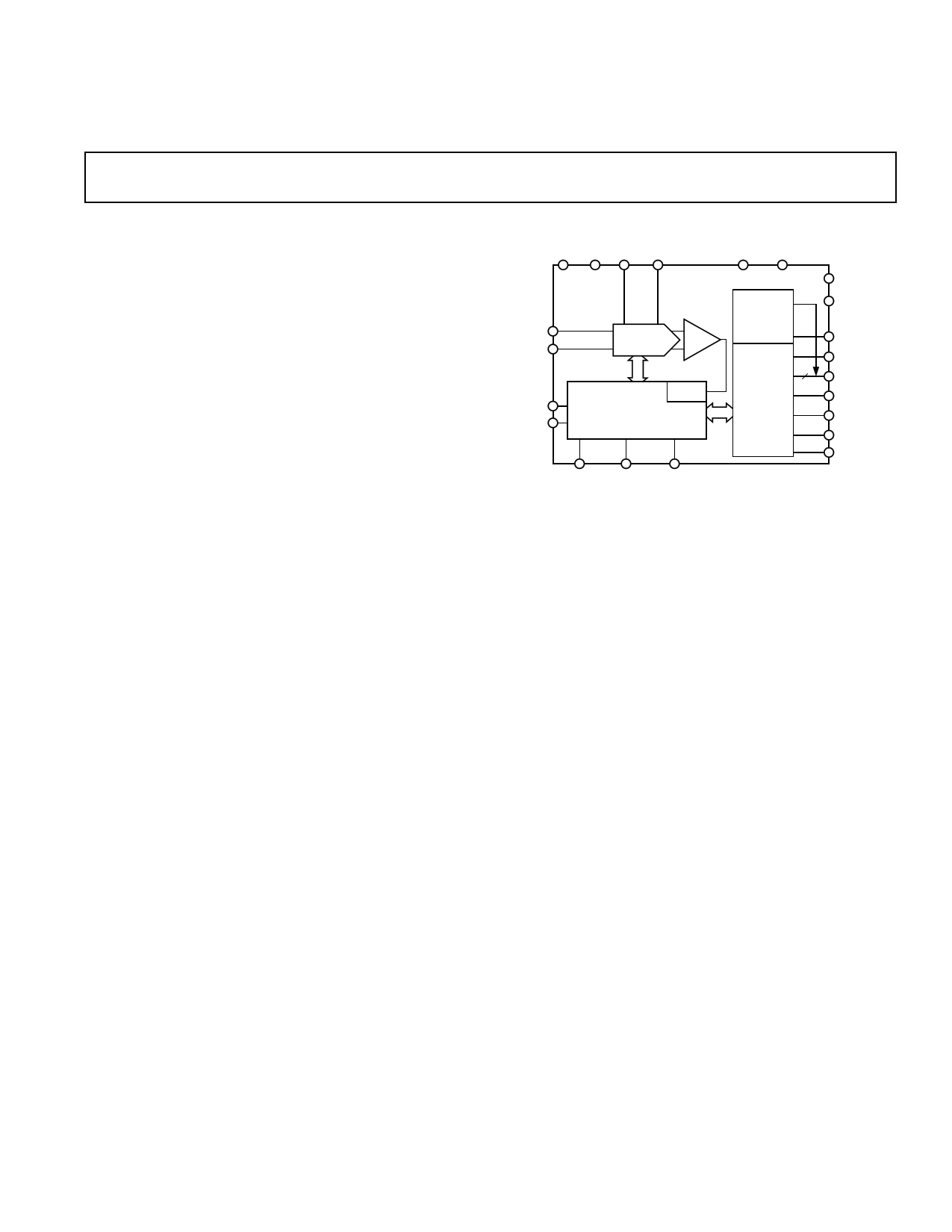
FUNCTIONAL BLOCK DIAGRAM
AVDD AGND REF REFGND
AD7677
IN+ SWITCHED
IN– CAP DAC
PD
RESET
CLOCK
CONTROL LOGIC AND
CALIBRATION CIRCUITRY
WARP IMPULSE CNVST
DVDD DGND
SERIAL
PORT
16
PARALLEL
INTERFACE
OVDD
OGND
SER/PAR
BUSY
DATA[15:0]
CS
RD
OB/2C
BYTESWAP
GENERAL DESCRIPTION
The AD7677 is a 16-bit, 1 MSPS, charge redistribution SAR,
fully differential, analog-to-digital converter that operates from a
single 5 V power supply. The part contains a high-speed 16-bit
sampling ADC, an internal conversion clock, error correction
circuits, and both serial and parallel system interface ports.
The AD7677 is hardware factory calibrated and comprehen-
sively tested to ensure such ac parameters as signal-to-noise
ratio (SNR) and total harmonic distortion (THD), in addition
to the more traditional dc parameters of gain, offset, and linearity.
It features a very high sampling rate mode (Warp) and, for
asynchronous conversion rate applications, a fast mode (Normal)
and, for low power applications, a reduced power mode (Impulse)
where the power is scaled with the throughput.
It is available in a 48-lead LQFP with operation specified from
–40°C to +85°C.
PRODUCT HIGHLIGHTS
1. Excellent INL
The AD7677 has a maximum integral nonlinearity of 1 LSB
with a no missing 16-bit code.
2. Superior AC Performances
The AD7677 has a minimum dynamic of 92 dB, 94 dB typical.
3. Fast Throughput
The AD7677 is a 1 MSPS, charge redistribution, 16-bit SAR
ADC with internal error correction circuitry.
4. Single-Supply Operation
The AD7677 operates from a single 5 V supply and typically
dissipates only 115 mW. Its power dissipation decreases
with the throughput. It consumes 7 µW maximum when in
power-down.
5. Serial or Parallel Interface
Versatile parallel (8 or 16 bits) or 2-wire serial interface
arrangement compatible with both 3 V or 5 V logic.
*Patent pending
REV. 0
Information furnished by Analog Devices is believed to be accurate and
reliable. However, no responsibility is assumed by Analog Devices for its
use, nor for any infringements of patents or other rights of third parties that
may result from its use. No license is granted by implication or otherwise
under any patent or patent rights of Analog Devices.
One Technology Way, P.O. Box 9106, Norwood, MA 02062-9106, U.S.A.
Tel: 781/329-4700
www.analog.com
Fax: 781/326-8703
© Analog Devices, Inc., 2001
1 page 
AD7677
Table I. Serial Clock Timings in Master Read after Convert
DIVSCLK[1]
DIVSCLK[0]
SYNC to SCLK First Edge Delay Minimum
Internal SCLK Period Minimum
Internal SCLK Period Maximum
Internal SCLK HIGH Minimum
Internal SCLK LOW Minimum
SDOUT Valid Setup Time Minimum
SDOUT Valid Hold Time Minimum
SCLK Last Edge to SYNC Delay Minimum
Busy High Width Maximum (Warp)
Busy High Width Maximum (Normal)
Busy High Width Maximum (Impulse)
t18
t19
t19
t20
t21
t22
t23
t24
t24
t24
t24
00 1
01 0
3 17 17
25 50 100
40 70 140
12 22 50
7 21 49
4 18 18
2 4 30
3 60 140
1.5 2
3
1.75 2.25 3.25
2 2.5 3.5
1
1 Unit
17 ns
200 ns
280 ns
100 ns
99 ns
18 ns
89 ns
300 ns
5.25 µs
5.55 µs
5.75 µs
ABSOLUTE MAXIMUM RATINGS1
Analog Inputs
IN+2, IN–2, REF, REFGND . . . . . . . . . . . . . . . . . . . . . . . .
. . . . . . . . . . . . . . . . . . . . AVDD + 0.3 V to AGND – 0.3 V
Ground Voltage Differences
AGND, DGND, OGND . . . . . . . . . . . . . . . . . . . . . ± 0.3 V
Supply Voltages
AVDD, DVDD, OVDD . . . . . . . . . . . . . . . . . . . . . . . . . 7 V
AVDD to DVDD, AVDD to OVDD . . . . . . . . . . . . . . ± 7 V
DVDD to OVDD . . . . . . . . . . . . . . . . . . . . . . . . . . . . . ± 7 V
Digital Inputs . . . . . . . . . . . . . . . . . –0.3 V to DVDD + 0.3 V
Internal Power Dissipation3 . . . . . . . . . . . . . . . . . . . . 700 mW
Junction Temperature . . . . . . . . . . . . . . . . . . . . . . . . . . 150°C
Storage Temperature Range . . . . . . . . . . . . –65°C to +150°C
Lead Temperature Range
(Soldering 10 sec) . . . . . . . . . . . . . . . . . . . . . . . . . . . 300°C
NOTES
1Stresses above those listed under Absolute Maximum Ratings may cause perma-
nent damage to the device. This is a stress rating only; functional operation of the
device at these or any other conditions above those indicated in the operational
section of this specification is not implied. Exposure to absolute maximum rating
conditions for extended periods may affect device reliability.
2See Analog Input section.
3Specification is for device in free air: 48-Lead LQFP: JA = 91°C/W, JC = 30°C/W.
1.6mA IOL
TO OUTPUT
PIN CL
60pF1
1.4V
500A IOH
NOTE
1IN SERIAL INTERFACE MODES,THE SYNC, SCLK, AND
SDOUT TIMINGS ARE DEFINED WITH A MAXIMUM LOAD
CL OF 10pF; OTHERWISE,THE LOAD IS 60pF MAXIMUM.
Figure 1. Load Circuit for Digital Interface Timing,
SDOUT, SYNC, SCLK Outputs, CL = 10 pF
0.8V
tDELAY
2V
0.8V
2V
tDELAY
2V
0.8V
Figure 2. Voltage Reference Levels for Timings
ORDERING GUIDE
Model
Temperature Range Package Description
Package Option
AD7677AST
AD7677ASTRL
EVAL-AD7677CB1
EVAL-CONTROL BRD22
–40°C to +85°C
–40°C to +85°C
Quad Flatpack (LQFP)
Quad Flatpack (LQFP)
Evaluation Board
Controller Board
ST-48
ST-48
NOTES
1This board can be used as a stand-alone evaluation board or in conjunction with the EVAL-CONTROL BRD2 for evaluation/
demonstration purposes.
2This board allows a PC to control and communicate with all Analog Devices evaluation boards ending in the CB designators.
CAUTION
ESD (electrostatic discharge) sensitive device. Electrostatic charges as high as 4000 V readily
accumulate on the human body and test equipment and can discharge without detection. Although
the AD7677 features proprietary ESD protection circuitry, permanent damage may occur on
devices subjected to high-energy electrostatic discharges. Therefore, proper ESD precautions are
recommended to avoid performance degradation or loss of functionality.
REV. 0
–5–
WARNING!
ESD SENSITIVE DEVICE
5 Page 
AD7677
250
DVDD
200
150
100
50 AVDD
OVDD
0
–55 –35 –15 5 25 45 65
TEMPERATURE – ؇C
85 105
TPC 13. Power-Down Operating Currents vs. Temperature
CIRCUIT INFORMATION
The AD7677 is a very fast, low-power, single-supply, precise,
16-bit analog-to-digital converter (ADC). The AD7677 features
different modes to optimize performances according to the
applications.
In Warp mode, the AD7677 is capable of converting 1,000,000
samples per second (1 MSPS).
The AD7677 provides the user with an on-chip track/hold,
successive approximation ADC that does not exhibit any pipe-
line or latency, making it ideal for multiple multiplexed channel
applications.
The AD7677 can be operated from a single 5 V supply and
be interfaced to either 5 V or 3 V digital logic. It is housed in a
48-lead LQFP package that combines space savings and flexible
configurations as either serial or parallel interface. The AD7677
is a pin-to-pin-compatible upgrade of the AD7664, AD7675,
and AD7676.
CONVERTER OPERATION
The AD7677 is a successive approximation analog-to-digital
converter based on a charge redistribution DAC. Figure 3 shows
the simplified schematic of the ADC. The capacitive DAC con-
sists of two identical arrays of 16 binary weighted capacitors
that are connected to the two comparator inputs.
During the acquisition phase, terminals of the array tied to the
comparator’s input are connected to AGND via SW+ and SW–.
All independent switches are connected to the analog inputs.
Thus, the capacitor arrays are used as sampling capacitors and
acquire the analog signal on IN+ and IN– inputs. When the
acquisition phase is complete and the CNVST input goes
low, a conversion phase is initiated. When the conversion phase
begins, SW+ and SW– are opened first. The two capacitor arrays
are then disconnected from the inputs and connected to the
REFGND input. Therefore, the differential voltage between the
inputs IN+ and IN– captured at the end of the acquisition phase
is applied to the comparator inputs, causing the comparator to
become unbalanced. By switching each element of the capacitor
array between REFGND or REF, the comparator input varies
by binary weighted voltage steps (VREF/2, VREF/4 . . . VREF/65536).
The control logic toggles these switches, starting with the MSB
first, in order to bring the comparator back into a balanced
condition. After the completion of this process, the control logic
generates the ADC output code and brings BUSY output low.
Modes of Operation
The AD7677 features three modes of operations, Warp, Normal,
and Impulse. Each of these modes is more suitable for specific
applications.
The Warp mode allows the fastest conversion rate up to 1 MSPS.
However, in this mode, and this mode only, the full specified accu-
racy is guaranteed only when the time between conversion does
not exceed 1 ms. If the time between two consecutive conversions
is longer than 1 ms, for instance, after power-up, the first conver-
sion result should be ignored. This mode makes the AD7677
ideal for applications where fast sample rates are required.
The Normal mode is the fastest mode (800 kSPS) without any
limitation about the time between conversions. This mode makes
the AD7677 ideal for asynchronous applications such as data
acquisition systems, where both high accuracy and fast sample
rate are required.
The Impulse mode, the lowest power dissipation mode, allows
power saving between conversions. The maximum throughput
in this mode is 666 kSPS. When operating at 100 SPS, for
example, it typically consumes only 15 µW. This feature makes
the AD7677 ideal for battery-powered applications.
IN+
REF
REFGND
IN–
MSB
32,768C 16,384C 4C 2C
32,768C 16,384C
MSB
4C 2C
LSB SW+
SWITCHES
CONTROL
CC
BUSY
COMP
CONTROL
LOGIC
OUTPUT
CODE
CC
LSB SW–
CNVST
Figure 3. ADC Simplified Schematic
REV. 0
–11–
11 Page | ||
| Páginas | Total 20 Páginas | |
| PDF Descargar | [ Datasheet AD7677.PDF ] | |
Hoja de datos destacado
| Número de pieza | Descripción | Fabricantes |
| AD767 | Microprocessor-Compatible 12-Bit D/A Converter | Analog Devices |
| AD7671 | 16-Bit 1 MSPS SAR Unipolar ADC with Ref | Analog Devices |
| AD7672 | HIGH-SPEED 12-BIT ADC | Analog Devices |
| AD7674 | 18-Bit/ 2.5 LSB INL/ 570 kSPS SAR ADC | Analog Devices |
| Número de pieza | Descripción | Fabricantes |
| SLA6805M | High Voltage 3 phase Motor Driver IC. |
Sanken |
| SDC1742 | 12- and 14-Bit Hybrid Synchro / Resolver-to-Digital Converters. |
Analog Devices |
|
DataSheet.es es una pagina web que funciona como un repositorio de manuales o hoja de datos de muchos de los productos más populares, |
| DataSheet.es | 2020 | Privacy Policy | Contacto | Buscar |