|
|
|
PDF AD976 Data sheet ( Hoja de datos )
| Número de pieza | AD976 | |
| Descripción | 16-Bit/ 100 kSPS/200 kSPS BiCMOS A/D Converters | |
| Fabricantes | Analog Devices | |
| Logotipo | ||
Hay una vista previa y un enlace de descarga de AD976 (archivo pdf) en la parte inferior de esta página. Total 16 Páginas | ||
|
No Preview Available !
a
FEATURES
Fast 16-Bit ADC
200 kSPS Throughput – AD976A
100 kSPS Throughput – AD976
Single 5 V Supply Operation
Input Range: ؎10 V
100 mW Max Power Dissipation
Choice of External or Internal 2.5 V Reference
High Speed Parallel Interface
On-Chip Clock
28-Lead Skinny DIP, SSOP or SOIC Packages
16-Bit, 100 kSPS/200 kSPS
BiCMOS A/D Converters
AD976/AD976A
CAP
VIN
AGND2
VDIG
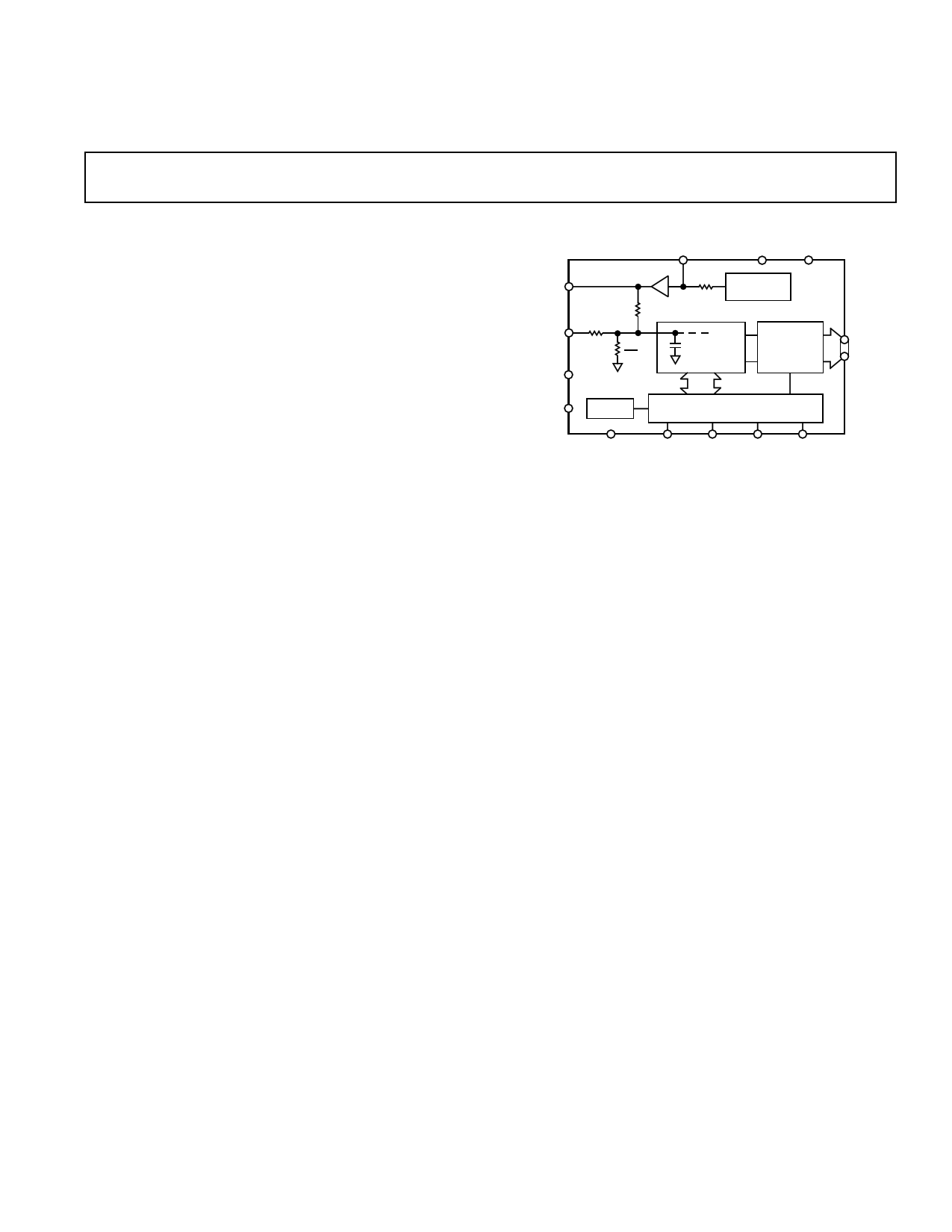
FUNCTIONAL BLOCK DIAGRAM
REF
VANA AGND1
R
4R
4R
3
4k⍀
2.5V
REFERENCE
AD976/AD976A
SWITCHED
CAP ADC
PARALLEL
INTERFACE
CLOCK
CONTROL LOGIC &
INTERNAL CALIBRATION CIRCUITRY
DGND
R = 6k⍀ AD976
R = 3k⍀ AD976A
BYTE
R/C
CS BUSY
D15
D0
GENERAL DESCRIPTION
The AD976/AD976A is a high speed, low power 16-bit A/D
converter that operates from a single 5 V supply. The part con-
tains a successive approximation, switched capacitor ADC, an
internal 2.5 V reference and a high speed parallel interface. The
ADC is factory calibrated to minimize all linearity errors. The
analog full-scale input is the standard industrial range of ± 10 V.
The AD976/AD976A is comprehensively tested for ac param-
eters such as SNR and THD, as well as the more traditional
parameters of offset, gain and linearity.
The AD976/AD976A is fabricated on Analog Devices’ propri-
etary BiCMOS process, which has high performance bipolar
devices along with CMOS transistors.
The AD976/AD976A is available in skinny 28-lead DIP, SSOP
and SOIC packages.
PRODUCT HIGHLIGHTS
1. Fast Throughput.
The AD976/AD976A is a high speed (100 kSPS/200 kSPS
throughput rates respectively), 16-bit ADC based on a
switched capacitor architecture.
2. Single-Supply Operation.
The AD976/AD976A operates from a single 5 V supply and
dissipates only 100 mW max.
3. Comprehensive DC and AC Specifications.
The AD976/AD976A is factory calibrated and fully tested for
SNR and THD as well as the traditional specifications of
offset, gain and linearity.
4. Complete A/D Solution.
The AD976/AD976A offers a highly integrated solution
containing an accurate ADC, reference and on-chip clock.
REV. C
Information furnished by Analog Devices is believed to be accurate and
reliable. However, no responsibility is assumed by Analog Devices for its
use, nor for any infringements of patents or other rights of third parties
which may result from its use. No license is granted by implication or
otherwise under any patent or patent rights of Analog Devices.
One Technology Way, P.O. Box 9106, Norwood, MA 02062-9106, U.S.A.
Tel: 781/329-4700 World Wide Web Site: http://www.analog.com
Fax: 781/326-8703
© Analog Devices, Inc., 1999
1 page 
ABSOLUTE MAXIMUM RATINGS1
Analog Inputs
VIN . . . . . . . . . . . . . . . . . . . . . . . . . . . . . . . . . . . . . . . ± 25 V
CAP . . . . . . . . . . . . . . . . +VANA + 0.3 V to AGND2 – 0.3 V
REF . . . . . . . . . . . . . . . . . . . . . Indefinite Short to AGND2
Ground Voltage Differences
DGND, AGND1, AGND2 . . . . . . . . . . . . . . . . . . . . ± 0.3 V
Supply Voltages
VANA . . . . . . . . . . . . . . . . . . . . . . . . . . . . . . . . . . . . . . . . 7 V
VDIG to VANA . . . . . . . . . . . . . . . . . . . . . . . . . . . . . . . . ± 7 V
VDIG . . . . . . . . . . . . . . . . . . . . . . . . . . . . . . . . . . . . . . . . 7 V
Digital Inputs . . . . . . . . . . . . . . . . . . . –0.3 V to VDIG + 0.3 V
Internal Power Dissipation2
PDIP (N), SOIC (R), SSOP (RS) . . . . . . . . . . . . . 700 mW
Junction Temperature . . . . . . . . . . . . . . . . . . . . . . . . . +150°C
Storage Temperature Range (N, R, RS) . . . –65°C to +150°C
Lead Temperature Range
(Soldering 10 sec) . . . . . . . . . . . . . . . . . . . . . . . . . . +300°C
NOTES
1Stresses above those listed under Absolute Maximum Ratings may cause perma-
nent damage to the device. This is a stress rating only; functional operation of the
device at these or any other conditions above those indicated in the operational
section of this specification is not implied. Exposure to absolute maximum rating
conditions for extended periods may affect device reliability.
2Specification is for device in free air:
28-Lead PDIP: θJA = 74°C/W; θJC = 24°C/W,
28-Lead SOIC: θJA = 72°C/W; θJC = 23°C/W,
28-Lead SSOP: θJA = 109°C/W; θJC = 39°C/W.
AD976/AD976A
PIN CONFIGURATION
DIP, SOIC and SSOP Packages
VIN 1
AGND1 2
REF 3
28 VDIG
27 VANA
26 BUSY
CAP 4
25 CS
AGND2 5
D15 (MSB) 6
AD976
AD976A
24 R/C
TOP VIEW 23 BYTE
D14 7 (Not to Scale) 22 D0 (LSB)
D13 8
21 D1
D12 9
20 D2
D11 10
19 D3
D10 11
18 D4
D9 12
17 D5
D8 13
16 D6
DGND 14
15 D7
1.6mA IOL
TO
OUTPUT
PIN
CL
100pF
500A IOH
+2.1V
Figure 1. Load Circuit for Digital Interface Timing
Model
AD976AN
AD976BN
AD976CN
AD976AAN
AD976ABN
AD976ACN
AD976AR
AD976BR
AD976CR
AD976AAR
AD976ABR
AD976ACR
AD976ARS
AD976BRS
AD976CRS
AD976AARS
AD976ABRS
AD976ACRS
Temperature
Range
–40°C to +85°C
–40°C to +85°C
–40°C to +85°C
–40°C to +85°C
–40°C to +85°C
–40°C to +85°C
–40°C to +85°C
–40°C to +85°C
–40°C to +85°C
–40°C to +85°C
–40°C to +85°C
–40°C to +85°C
–40°C to +85°C
–40°C to +85°C
–40°C to +85°C
–40°C to +85°C
–40°C to +85°C
–40°C to +85°C
Max
INL
± 3.0 LSB
± 2.0 LSB
± 3.0 LSB
± 2.0 LSB
± 3.0 LSB
± 2.0 LSB
± 3.0 LSB
± 2.0 LSB
± 3.0 LSB
± 2.0 LSB
± 3.0 LSB
± 2.0 LSB
ORDERING GUIDE
Min
S/(N+D)
83 dB
85 dB
83 dB
83 dB
85 dB
83 dB
83 dB
85 dB
83 dB
83 dB
85 dB
83 dB
83 dB
85 dB
83 dB
83 dB
85 dB
83 dB
Throughput
Rate
100 kSPS
100 kSPS
100 kSPS
200 kSPS
200 kSPS
200 kSPS
100 kSPS
100 kSPS
100 kSPS
200 kSPS
200 kSPS
200 kSPS
100 kSPS
100 kSPS
100 kSPS
200 kSPS
200 kSPS
200 kSPS
Package
Descriptions
Package
Options
28-Lead, 300 mil Plastic DIP
28-Lead, 300 mil Plastic DIP
28-Lead, 300 mil Plastic DIP
28-Lead, 300 mil Plastic DIP
28-Lead, 300 mil Plastic DIP
28-Lead, 300 mil Plastic DIP
28-Lead Small Outline Package
28-Lead Small Outline Package
28-Lead Small Outline Package
28-Lead Small Outline Package
28-Lead Small Outline Package
28-Lead Small Outline Package
28-Lead Shrink Small Outline Package
28-Lead Shrink Small Outline Package
28-Lead Shrink Small Outline Package
28-Lead Shrink Small Outline Package
28-Lead Shrink Small Outline Package
28-Lead Shrink Small Outline Package
N-28B
N-28B
N-28B
N-28B
N-28B
N-28B
R-28
R-28
R-28
R-28
R-28
R-28
RS-28
RS-28
RS-28
RS-28
RS-28
RS-28
CAUTION
ESD (electrostatic discharge) sensitive device. Electrostatic charges as high as 4000 V readily
accumulate on the human body and test equipment and can discharge without detection.
Although the AD976/AD976A features proprietary ESD protection circuitry, permanent damage
may occur on devices subjected to high energy electrostatic discharges. Therefore, proper ESD
precautions are recommended to avoid performance degradation or loss of functionality.
REV. C
–5–
WARNING!
ESD SENSITIVE DEVICE
5 Page 
AD976/AD976A
VOLTAGE REFERENCE
The AD976/AD976A has an on-chip temperature compensated
bandgap voltage reference that is factory trimmed to 2.5 V
± 20 mV. The full-scale range of the ADC is equal to ± 4 VREF.
Thus, the nominal range will be ± 10 V.
The accuracy of the AD976 over the specified temperature
range is dominated by the drift performance of the voltage refer-
ence. The on-chip voltage reference is laser-trimmed to provide
a typical drift of 7 ppm/°C. This typical drift characteristic is
shown in Figure 13, which is a plot of the change in reference
voltage (in mV) versus the change in temperature—notice the
plot is normalized for zero error at +25°C. If improved drift
performance is required, an external reference such as the
AD780 should be used to provide a drift as low as 3 ppm/°C. In
order to simplify the drive requirements of the voltage reference
(internal or external), an onboard reference buffer is provided.
The output of this buffer is provided at the CAP pin and is
available to the user; however, when externally loading the refer-
ence buffer, it is important to make sure that proper precautions
are taken to minimize any degradation in the ADC’s perfor-
mance. Figure 14 shows the load regulation of the reference
buffer. Notice that this figure is also normalized so that there is
zero error with no dc load. In the linear region, the output im-
pedance at this point is typically 1 ohm. Because of this 1 ohm
output impedance, it is important to minimize any ac or input
dependent loads that will lead to increased distortion. Any dc
loads will simply act as a gain error. Although the typical char-
acteristic of Figure 14 shows that the AD976 is capable of driv-
ing loads greater than 15 mA, it is not recommended that the
steady state current exceed 2 mA.
In addition to the on-chip reference, an external 2.5 V reference
can be applied. When choosing an external reference for a
16-bit application, however, careful attention should be paid to
noise and temperature drift. These critical specifications can
have a significant effect on the ADC performance.
Figure 9 shows the AD976/AD976A with the AD780 voltage
reference applied to the REF pin. The AD780 is a bandgap
reference that exhibits ultralow drift, low initial error, and low
output noise. For low power applications, the REF192 provides
a low quiescent current, high accuracy and low temperature
drift solution.
0.1F
+5V
؎10V INPUT
TEMP VOUT
AD780
VIN GND
R1
200⍀
R2
33.2k⍀
C1
2.2F
C3 C4
1F 0.1F
C2
2.2F
VIN
REF AD976/
AD976A
AGND1
VANA
CAP
AGND2
Figure 9. AD780 External Reference Connection to the
AD976/AD976A
AC PERFORMANCE
The AD976/AD976A is fully specified and tested for dynamic
performance specifications. The ac parameters are required for
signal processing applications such as speech recognition and
spectrum analysis. These applications require information on
the ADC’s effect on the spectral content of the input signal.
Hence, the parameters for which the AD976/AD976A is
specified include: S/(N+D), THD and Spurious Free Dynamic
Range. These terms are discussed in greater detail in the follow-
ing sections.
As a general rule, it is recommended that the results from sev-
eral conversions be averaged to reduce the effects of noise, thus
improving parameters such as S/(N+D) and THD. The ac per-
formance of the AD976/AD976A can be optimized by operating
the ADC at its maximum sampling rate of 100 kHz/200 kHz
and by digitally filtering the resulting bit stream to the desired
signal bandwidth. By distributing noise over a wider frequency
range, the noise density in the frequency band of interest can be
reduced. For example, if the required input bandwidth is 50 kHz,
the AD976A could be oversampled by a factor of 2. This would
yield a 3 dB improvement in the effective SNR performance.
100%
0
–10
–20 FSAMPLE = 200kHz
–30 FIN = 45kHz
SNR = 86.23dB
–40 THD = –105.33dB
–50
–60
–70
–80
–90
–100
–110
–120
–130
–140
–150
0 5 10 15 20 25 30 35 40 45 50 55 60 65 70 75 80 85 90 95100
FREQUENCY – kHz
Figure 10. FFT PLOT
DC PERFORMANCE
The factory calibration scheme used for the AD976/AD976A
compensates for bit weight errors that may exist in the capacitor
array. The mismatch in capacitor values is adjusted (using the
calibration coefficients) during a conversion, resulting in excellent
dc linearity performance. Figures 11, 12, 15, 16, 17 and 18,
respectively, show typical INL, typical DNL, typical positive and
negative INL and DNL distribution plots for the AD976/AD976A
at +25°C.
A histogram test is a statistical method for deriving an A/D
converter’s differential nonlinearity. A ramp input is sampled
by the ADC and a large number of conversions are taken and
stored. Theoretically, the codes would all be the same size and
therefore have an equal number of occurrences. A code with an
average number of occurrences would have a DNL of “0.” A
code that is different than the average would have a DNL that
was either greater or less than zero LSB. A DNL of –1 LSB
indicates that there is a missing code present at the 16-bit level
and that the ADC exhibits 15-bit performance.
REV. C
–11–
11 Page | ||
| Páginas | Total 16 Páginas | |
| PDF Descargar | [ Datasheet AD976.PDF ] | |
Hoja de datos destacado
| Número de pieza | Descripción | Fabricantes |
| AD9700 | Video Dispaly D/A Converter | ETC |
| AD9700 | Monolithic Video D/A Converter | Analog Devices |
| AD9701 | 250 MSPS Video Digital-to-Analog Converter | Analog Devices |
| AD9702 | Triple 4-Bit D/A Converter | Analog Devices |
| Número de pieza | Descripción | Fabricantes |
| SLA6805M | High Voltage 3 phase Motor Driver IC. |
Sanken |
| SDC1742 | 12- and 14-Bit Hybrid Synchro / Resolver-to-Digital Converters. |
Analog Devices |
|
DataSheet.es es una pagina web que funciona como un repositorio de manuales o hoja de datos de muchos de los productos más populares, |
| DataSheet.es | 2020 | Privacy Policy | Contacto | Buscar |